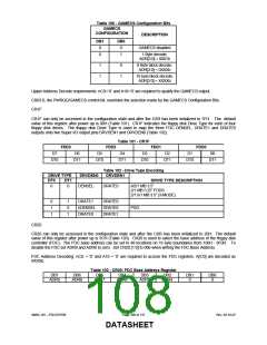
Table 100 - GAMECS Configuration Bits
GAMECS
CONFIGURATION
DESCRIPTION
DB1
0
DB0
0
GAMECS disabled
0
1
1 Byte decode,
ADR[3:0] = 0001b
1
1
0
1
8 Byte block decode,
ADR[3:0] = 0XXXb
16 byte block decode,
ADR[3:0] = XXXXb
Upper Address Decode requirements: nCS=’0’ and A10=’0’ are required to qualify the GAMECS output.
CR03.0, the PWRGD/GAMECS control bit, overrides the selection made by the GAMECS Configuration Bits.
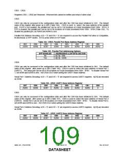
CR1F
CR1F can only be accessed in the configuration state and after the CSR has been initialized to 1FH. The default
value of this register after power up is 00H (Table 101). CR1F indicates the floppy disk Drive Type for each of four
floppy disk drives. The floppy disk Drive Type is used to map the three FDC DENSEL, DRATE1 and DRATE0
outputs onto two Super I/O output pins DRVDEN1 and DRVDEN0 (Table 102).
Table 101 - CR1F
FDD3
FDD2
FDD1
FDD0
D7
D6
D5
D4
D3
D2
D1
D0
DT0
DT1
DT0
DT1
DT0
DT1
DT0
DT1
Table 102 - Drive Type Encoding
DRVDEN1
DRIVE TYPE
DRVDEN0
DT0
DT1
DRIVE TYPE DESCRIPTION
0
0
DENSEL
DRATE0
4/2/1 MB 3.5”
2/1 MB 5.25” FDDS
2/1.6/1 MB 3.5” (3-MODE)
0
1
1
1
0
1
DRATE1
nDENSEL
DRATE0
DRATE0
DRATE0
DRATE1
PS/2
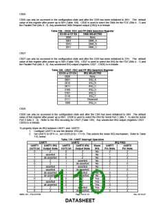
CR20
CR20 can only be accessed in the configuration state and after the CSR has been initialized to 20H. The default
value of this register after power up is 3CH (Table 103). CR20 is used to select the base address of the floppy disk
controller (FDC). The FDC base address can be set to 48 locations on 16 byte boundaries from 100H - 3F0H. To
disable the FDC set ADR9 and ADR8 to zero. Set CR20.[1:0] to 00b when writing the FDC Base Address.
FDC Address Decoding: nCS = ’0’ and A10 = ’0’ are required to access the FDC registers. A[3:0] are decoded as
0XXXb.
Table 103 - CR20: FDC Base Address Register
DB7
ADR9
DB6
ADR8
DB5
ADR7
DB4
ADR6
DB3
ADR5
DB2
ADR4
DB1
0
DB0
0
SMSC DS – FDC37N769
Page 108 of 137
Rev. 02-16-07
DATASHEET

 SMSC [ SMSC CORPORATION ]