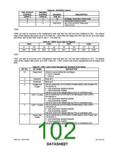
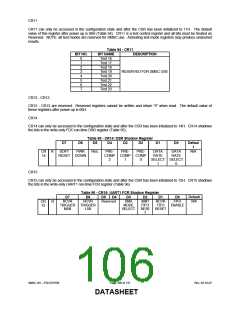
CR11
CR11 can only be accessed in the configuration state and after the CSR has been initialized to 11H. The default
value of this register after power up is 80H (Table 94). CR11 is a test control register and all bits must be treated as
Reserved. NOTE: all test modes are reserved for SMSC use. Activating test mode registers may produce undesired
results.
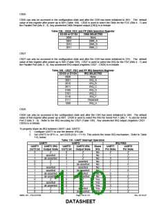
Table 94 - CR11
BIT NO.
BIT NAME
Test 16
Test 17
Test 18
Test 19
Test 20
Test 21
Test 22
Test 23
DESCRIPTION
0
1
2
3
4
5
6
7
RESERVED FOR SMSC USE
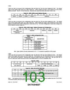
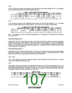
CR12 - CR13
CR12 - CR13 are reserved. Reserved registers cannot be written and return “0” when read. The default value of
these registers after power up is 00H.
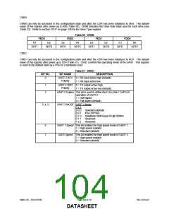
CR14
CR14 can only be accessed in the configuration state and after the CSR has been initialized to 14H. CR14 shadows
the bits in the write-only FDC run-time DSR register (Table 95).
Table 95 - CR14: DSR Shadow Register
D7
D6
D5
D4
D3
D2
D1
D0
Defaul
t
CR
14
R
SOFT
RESET DOWN
PWR
Res.
PRE-
PRE-
PRE-
DATA
RATE
DATA
RATE
N/A
COMP COMP COMP
2
1
0
SELECT SELECT
1
0
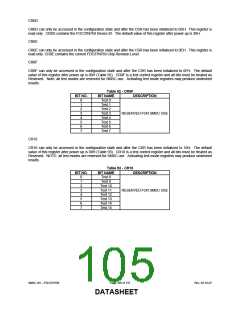
CR15
CR15 can only be accessed in the configuration state and after the CSR has been initialized to 15H. CR15 shadows
the bits in the write-only UART1 run-time FCR register (Table 96).
Table 96 - CR15: UART1 FCR Shadow Register
Default
N/A
D7
RCVR
TRIGGER
MSB
D6
RCVR
TRIGGER
LSB
D5
Reserved
D4
D3
DMA
MODE
SELECT
D2
XMIT
FIFO
RESE
T
D1
RCVR
FIFO
D0
FIFO
ENABLE
CR
15
R
RESET
SMSC DS – FDC37N769
Page 106 of 137
Rev. 02-16-07
DATASHEET

 SMSC [ SMSC CORPORATION ]