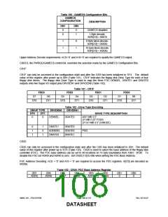
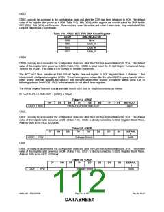
CR2C
CR2C can only be accessed in the configuration state and after the CSR has been initialized to 2CH. The default
value of this register after power up is 00H (Table 113). Bits D[3:0] of this register are used to select the DMA for the
SCE (FIR). Bits D[7:4] are Reserved. Reserved bits cannot be written and return 0 when read. Any unselected DMA
Request output (DRQ) is in tristate.
Table 113 - CR2C: SCE (FIR) DMA Select Register
D3-D0
0000
0001
0010
0011
DMA SELECTED
None
DMA_A
DMA_B
DMA_C
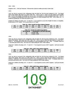
CR2D
CR2D can only be accessed in the configuration state and after the CSR has been initialized to 2DH. The default
value of this register after power up is 03H (Table 114). CR2D is used to set the IR Half Duplex Turnaround Delay
Time for the IR port. This value is 0 to 10msec in 100µsec increments.
The IRCC v2.0 block includes an 8 bit IR Half Duplex Time-out register in SCE Register Block 5, Address 1 that
interacts with configuration register CR2D. These two registers behave like the other IRCC Legacy controls where
either source uniformly updates the value of both registers when either register is explicitly written using IOW or
following a device-level POR. IRCC software resets do not affect these registers.
The IR Half Duplex Time-out is programmable from 0 to 25.5mS in 100μS increments, as follows:
IR HALF DUPLEX TIME-OUT = (CR2D) x 100μS
Table 114 - CR2D
D7
D6
D5
D4
D3
D2
D1
D0
DEFAULT
CR2D R/W
IR HALF DUPLEX TIME-OUT
0x03
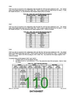
CR2E
CR2E can only be accessed in the configuration state and after the CSR has been initialized to 2EH. The default
value of this register after power up is 00H (Table 115). CR2E is directly connected to SCE Register Block Three,
Address 0x05 in the IRCC v2.0 block.
Table 115 - CR2E
D7
D6
D5
D4
D3
D2
D1
D0
DEFAUL
T
CR2E
R/W
Software Select A
0x00
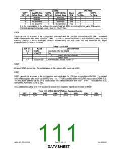
CR2F
CR2F can only be accessed in the configuration state and after the CSR has been initialized to 2FH. The default
value of this register after power up is 00H (Table 116). CR2F is directly connected to SCE Register Block Three,
Address 0x06 in the IRCC v2.0 block.
Table 116 - CR2F
D7
D6
D5
D4
D3
D2
D1
D0
DEFAUL
T
CR2F
R/W
Software Select B
0x00
SMSC DS – FDC37N769
Page 112 of 137
Rev. 02-16-07
DATASHEET

 SMSC [ SMSC CORPORATION ]