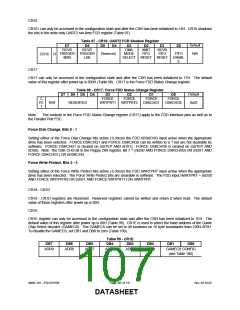
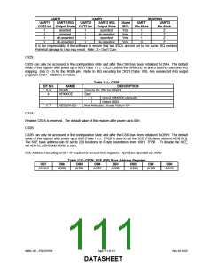
CR16
CR161 can only be accessed in the configuration state and after the CSR has been initialized to 16H. CR16 shadows
the bits in the write-only UART2 run-time FCR register (Table 97).
Table 97 - CR16: UART2 FCR Shadow Register
Default
N/A
D7
RCVR
TRIGGER TRIGGER
MSB LSB
D6
RCVR
D5
D4
D3
DMA
MODE
SELECT
D2
XMIT
FIFO
D1
RCVR
FIFO
D0
Reserved
FIFO
ENABL
E
CR16
R
RESET RESET
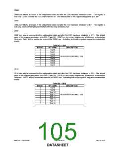
CR17
CR17 can only be accessed in the configuration state and after the CSR has been initialized to 17H. The default
value of this register after power up is 003H (Table 98). CR17 is the Force FDD Status Change register.
Table 98 - CR17: Force FDD Status Change Register
Default
0x03
D7 D6 D5 D4
D3
FORCE
WRTPRT1
D2
FORCE
WRTPRT0
D1
FORCE
DSKCHG1
D0
FORCE
DSKCHG0
C
R1
7
R/W
RESERVED
Note:
The controls in the Force FDD Status Change register (CR17) apply to the FDD Interface pins as well as to
the Parallel Port FDC.
Force Disk Change, Bits 0 - 1
Setting either of the Force Disk Change bits active (1) forces the FDD nDSKCHG input active when the appropriate
drive has been selected. FORCE DSKCHG1 and FORCE DSKCHG0 can be written to a 1 but are not clearable by
software. FORCE DSKCHG1 is cleared on (nSTEP AND nDS1), FORCE DSKCHG0 is cleared on (nSTEP AND
nDS0). Note: The DSK CHG bit in the Floppy DIR register, Bit 7 = (nDS0 AND FORCE DSKCHG0) OR (nDS1 AND
FORCE DSKCHG1) OR nDSKCHG.
Force Write Protect, Bits 2 - 3
Setting either of the Force Write Protect bits active (1) forces the FDD nWRTPRT input active when the appropriate
drive has been selected. The Force Write Protect bits are clearable in software. The FDD input nWRTPRT = (nDS0
AND FORCE WRTPRT0) OR (nDS1 AND FORCE WRTPRT1) OR nWRTPRT.
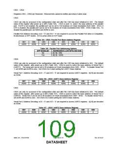
CR18 - CR1D
CR18 - CR1D registers are Reserved. Reserved registers cannot be written and return 0 when read. The default
value of these registers after power up is 00H.
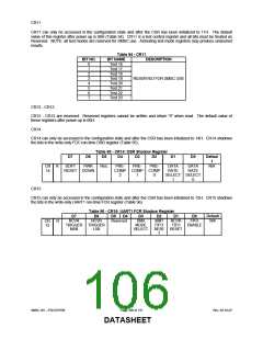
CR1E
CR1E register can only be accessed in the configuration state and after the CSR has been initialized to 1EH. The
default value of this register after power up is 80H (Table 99). CR1E is used to select the base address of the Game
Chip Select decoder (GAMECS). The GAMECS can be set to 48 locations on 16 byte boundaries from 100H-3F0H.
To disable the GAMECS, set DB1 and DB0 to zero (Table 100).
Table 99 - CR1E
DB7
DB6
DB5
DB4
DB3
DB2
DB1
DB0
ADR9
ADR8
ADR7
ADR6
ADR5
ADR4
GAMECS CONFIG
(see Table 100)
SMSC DS – FDC37N769
Page 107 of 137
Rev. 02-16-07
DATASHEET

 SMSC [ SMSC CORPORATION ]