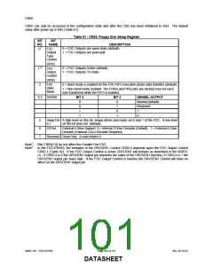
CR0D
CR0D can only be accessed in the configuration state and after the CSR has been initialized to 0DH. This register is
read only. CR0D contains the FDC37N769 Device ID. The default value of this register after power up is 28H.
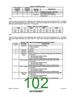
CR0E
CR0E can only be accessed in the configuration state and after the CSR has been initialized to 0EH. This register is
read only. CR0E contains the current FDC37N769 Chip Revision Level.
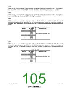
CR0F
CR0F can only be accessed in the configuration state and after the CSR has been initialized to 0FH. The default
value of this register after power up is 00H (Table 92). CR0F is a test control register and all bits must be treated as
Reserved. Note: all test modes are reserved for SMSC use. Activating test mode registers may produce undesired
results.
Table 92 - CR0F
BIT NO.
BIT NAME
Test 0
Test 1
Test 2
Test 3
Test 4
Test 5
Test 6
Test 7
DESCRIPTION
0
1
2
3
4
5
6
7
RESERVED FOR SMSC USE
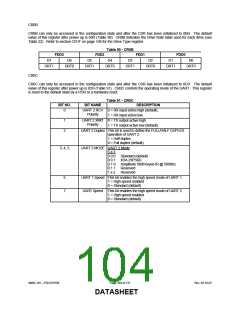
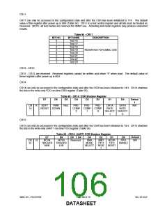
CR10
CR10 can only be accessed in the configuration state and after the CSR has been initialized to 10H. The default
value of this register after power up is 00H (Table 93). CR10 is a test control register and all bits must be treated as
Reserved. NOTE: all test modes are reserved for SMSC use. Activating test mode registers may produce undesired
results.
Table 93 - CR10
BIT NO.
BIT NAME
Test 8
Test 9
Test 10
Test 11
Test 12
Test 13
Test 14
Test 15
DESCRIPTION
0
1
2
3
4
5
6
7
RESERVED FOR SMSC USE
SMSC DS – FDC37N769
Page 105 of 137
Rev. 02-16-07
DATASHEET

 SMSC [ SMSC CORPORATION ]