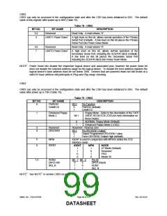
CR08
CR08 can only be accessed in the configuration state and after the CSR has been initialized to 08H. The default
value of this register after power up is 00H (Table 85). CR08 contains the lower 4 bits (ADRA7:4) for the ADRx
address decoder. Bits D0 - D3 are Reserved. Reserved bits cannot be written and return 0 when read.
Table 85 - CR08: ADRx Lower Address Decode
D7
D6
D5
D4
D3
D2
D1
D0
ADRA7
ADRA6
ADRA5
ADRA4
Reserved
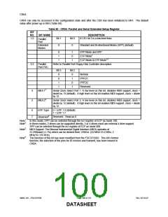
CR09
CR09 can only be accessed in the configuration state and after the CSR has been initialized to 09H. The default
value of this register after power up is 00H (Table 86). CR09 contains the upper 3 bits (ADRA10:8) of the ADRx
address decoder and the ADRx Configuration Control Bits D[7:6]. The ADRx Configuration Control Bits configure the
ADRx Address Decoder (Table 87).
Table 86 - CR09: ADRx Upper Address Decoder and Configuration
D7
D6
D5
D4
D3
D2
D1
D0
ADRx
Reserved
ADRA10
ADRA9
ADRA8
CONFIGURATION
CONTROL
Table 87 - ADRx Configuration Bits
ADRx
CONFIGURATION
CONTROL
DESCRIPTION
D7
0
0
D6
0
1
ADRx disabled
1 Byte decode
A[3:0]=0000b
1
1
0
1
8 Byte block decode
A[3:0]=0XXXb
16 byte block decode
A[3:0]=XXXXb
Note: Upper Address Decode requirements: nCS = ’0’ is required to qualify the ADRx output.
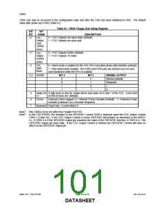
CR0A
CR0A can only be accessed in the configuration state and after the CSR has been initialized to 0AH. The default
value of this register after power up is 00H (Table 88). CR0A defines the FIFO threshold for the ECP mode parallel
port. Bits D[5:4] are Reserved. Reserved Bits cannot be written and return 0 when read. Bits D[7:6] are the IR
OUTPUT MUX bits (Table 89) and are reset to the default state by a POR or a hardware reset.
Table 88 - CR0A
D7
D6
D5
D4
D3
D2
ECP FIFO THRESHOLD
THR2 THR1
D1
D0
IR OUTPUT MUX
(see Table 89)
RESERVED
THR3
THR0
Table 89 - CR0A: IR OUTPUT MUX Bits
D7
0
D6
0
Mux Mode
Active device to COM port (Default). That is, use pins IRRX and IRTX
(pins 88 and 89).
0
1
1
1
0
1
Active device to IR port. That is, use IRRX2, IRTX2 (pins 23, 24)
Reserved.
Outputs Inactive: IRTX and IRTX2 are High-Z.
Note:
The function of the IR OUTPUT MUX bits and how they are reset has been modified from the FDC37C669.
The first two options were previously selected through CR04.
SMSC DS – FDC37N769
Page 103 of 137
Rev. 02-16-07
DATASHEET

 SMSC [ SMSC CORPORATION ]