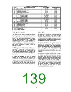
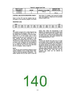
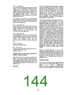
Table 65 - Update Cycle Time
INPUT CLOCK
FREQUENCY
32.768 kHz
MINIMUM TIME
UPDATE CYCLE
UIP BIT
UPDATE CYCLE TIME
1
0
-
1948 μs
32.768 kHz
-
244 μs
when Bank 0 is enabled, even during the update
cycle. Note Register D, Bits[6:0] are not accessible
during an update cycle.
CONTROL AND STATUS REGISTERS, BANK 0
Bank 0 of the RTC has five registers that are
accessible to the processor program at all times
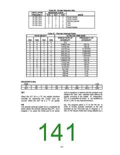
REGISTER A (AH)
MSB
LSB
b7
b6
b5
b4
b3
b2
b1
b0
UIP
DV2
DV1
DV0
RS3
RS2
RS1
RS0
divider chain. When the time/calendar is first
initialized, the program may start the divider chain
at the precise time stored in the registers. When
the divider reset is removed the first update begins
one-half second later. These three read/write bits
are not affected by RESET_DRV.
UIP
The update in progress bit is a status flag that may
be monitored by the program. When UIP is a "1"
the update cycle is in progress or will soon begin.
When UIP is a "0" the update cycle is not in
progress and will not be for at least 244 μs. The
time, calendar, and alarm information is fully
available to the program when the UIP bit is zero.
The UIP bit is a read- only bit and is not affected
by RESET_DRV. Writing the SET bit in Register B
to a "1" inhibits any update cycle and then clears
the UIP status bit. The UIP bit is only valid when
the RTC is enabled. Refer to Table 66.
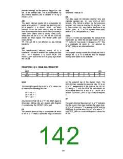
RS3-0
The four rate selection bits select one of 15 taps
on the divider chain or disable the divider output.
The selected tap determines rate or frequency of
the periodic interrupt. The program may enable or
disable the interrupt with the PIE bit in Register B.
Table 67 lists the periodic interrupt rates and
equivalent output frequencies that may be chosen
with the RS0-RS3 bits. These four bits are
read/write bits, which are not affected by
RESET_DRV.
DV2-0
Three bits are used to permit the program to select
various conditions of the 22-stage divider chain.
Table 66 shows the allowable combinations. The
divider selection bits are also used to reset the
111

 SMSC [ SMSC CORPORATION ]