register, Input Data register, and Output Data
register. Table 61 shows how the interface
decodes the control signals. In addition to the
above signals, the host interface includes
keyboard and mouse IRQs.
RTC INTERFACE
The ISA interface is functionally compatible with
the 8042-style host interface. It consists of the D0-
7 data bus, the nIOR, nIOW and the Status
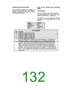
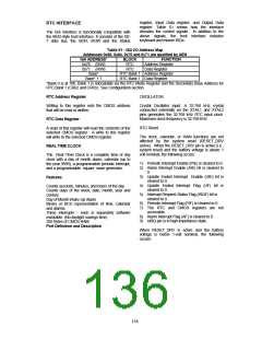
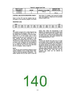
Table 61 - ISA I/O Address Map
Addresses 0x60, 0x64, 0x70 and 0x71 are qualified by AEN
ISA ADDRESS*
0x70 (R/W)
0x71 (R/W)
Base*
BLOCK
RTC
RTC
RTC Bank 1 Address Register
RTC Bank 1 Data Register
FUNCTION
Address Register
Data Register
Base* + 1
*Bank 0 is at 70h. Bank 1 is relocatable via the RTC Mode Register and the Secondary Base Address for
RTC Bank 1 (CR62 and CR63). See Configuration section.
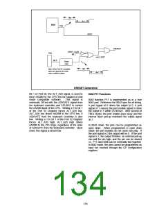
OSCILLATOR
RTC Address Register
Crystal Oscillator input. A 32.768 kHz crystal
connected externally on the XTAL1 and XTAL2
pins generates the 32.768 kHz RTC input clock.
Maximum clock frequency is 32.768 KHz.
Writing to this register sets the CMOS address
that will be read or written.
RTC Data Register
RTC Reset
A read of this register will read the contents of the
selected CMOS register. A write to this register
will write to the selected CMOS register.
The clock, calendar, or RAM functions are not
affected by the system reset (RESET_DRV
active). When the RESET_DRV pin is active (i.e.,
system reset) and the battery voltage is above 1
volt nominal, the following occurs:
REAL TIME CLOCK
The Real Time Clock is a complete time of day
clock with a day of month alarm, calendar (up to
the year 9999), a programmable periodic interrupt,
and a programmable square wave generator.
1) Periodic Interrupt Enable (PIE) is cleared to 0.
2) Alarm Interrupt Enable (AIE) bit is cleared to
0.
3) Update Ended Interrupt Enable (UIE) bit is
cleared to 0.
Features
4) Update Ended Interrupt Flag (UF) bit is
cleared to 0.
5) Interrupt Request Status Flag (IRQF) bit is
cleared to 0.
Counts seconds, minutes, and hours of the day.
Counts days of the week, date, month, year and
century.
Day of Month Wake-Up Alarm
6) Periodic Interrupt Flag (PIF) is cleared to 0.
7) The RTC and CMOS registers are not
accessible.
8) Alarm Interrupt Flag (AF) is cleared to 0.
9) nIRQ pin is in high impedance state.
Binary or BCD representation of time, calendar
and alarms.
Three interrupts - each is separately software
maskable. (No daylight savings time)
256 Bytes of CMOS RAM.
Port Definition and Description
When RESET_DRV is active and the battery
voltage is below 1-volt nominal, the following
occurs:
138

 SMSC [ SMSC CORPORATION ]