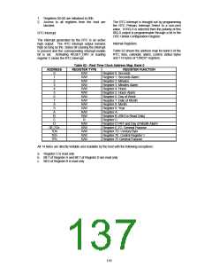
Table 63 shows Bank 1, the second bank of
CMOS registers which contains an additional 128
bytes of general purpose CMOS registers.
All 128 bytes are directly writeable and readable
by the host.
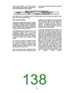
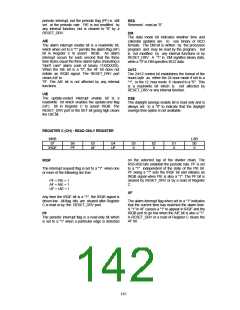
Table 63 - Real Time Clock Address Map, Bank 1
ADDRESS
REGISTER TYPE
REGISTER FUNCTION
0-7F
R/W
Register 0-7F: General Purpose
Note: CMOS Bank 1 is relocatable via the RTC Mode Register and the Secondary Base Address (CR62
and CR63). See Configuration Section.
update logic to be advanced by one second and to
check for an alarm condition. If any of these bytes
are read at this time, the data outputs are
undefined. The update cycle time is shown in
Table 65. The update logic contains circuitry for
automatic end-of-month recognition as well as
automatic leap year compensation.
Time, Calendar and Alarm
The processor program obtains time and calendar
information by reading the appropriate locations.
The program may initialize the time, calendar and
alarm by writing to these locations. The contents of
the time, calendar, century and alarm bytes can be
in binary or BCD as shown in Table 64.
An alarm can be generated for day of month, day,
hour, minute, or seconds. The alarm may be used
in two ways. First, when the program inserts an
alarm time in the appropriate date, hours, minutes
and seconds alarm locations, the alarm interrupt is
initiated at the specified time each day if the alarm
enable bit is high. The second usage is to insert a
"don't care" state in one or more of three alarm
bytes. The "don't care" code is any hexadecimal
byte from C0 to FF inclusive. That is the two most
significant bits of each byte, when set to "1", create
a "don't care" situation. An alarm interrupt each
hour is created with a "don't care" code in the
hours and date alarm location. Similarly, an alarm
is generated every minute with "don't care" codes
in the hours, date and minutes alarm bytes. The
"don't care" codes in all three alarm bytes create
Before initializing the internal registers, the SET bit
in Register B should be set to a "1" to prevent
time/calendar updates from occurring. The
program initializes the ten locations in the binary or
BCD format as defined by the DM bit in Register
B. The SET bit may now be cleared to allow
updates.
The 12/24 bit in Register B establishes whether
the hour locations represent 1 to 12 or 0 to 23.
The 12/24 bit cannot be changed without
reinitializing the hour locations. When the 12 hour
format is selected, the high order bit of the hours
byte represents PM when it is a "1".
Once per second, the time, calendar and alarm
bytes, as well as the century byte switched to the
an
interrupt
every
second.
140

 SMSC [ SMSC CORPORATION ]