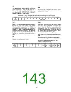
BIT 0 - AL_REM_EN
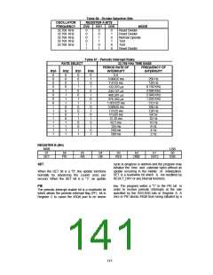
The RTC includes three separate fully- automatic
sources of interrupts to the processor. The alarm
interrupt may be programmed to occur at rates
from one-per-second to one-a-day. The periodic
One of the two control bits for the alarm wakeup
function; it is the “remember” enable bit for the
second alarm. This bit, if set to 1, wil cause the
system to power-up upon return of power if the
alarm 2 time has passed during loss of power. It is
only applicable when VTR=0.
independent of the other control bit for the alarm
wake-up function, AlE.
interrupt
may be selected for rates from
half-a-second to 122.070 μs. The update ended
interrupt may be used to indicate to the program
that an update cycle is completed. Each of
these independent interrupts are described in
greater detail in other sections.
This bit is
If AL_REM_EN is set and VTR=0 at the date/time
that the alarm is set for, the nPowerOn pin will go
active (low) and the machine will power-up as
soon as VTR comes back.
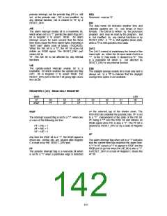
The processor program selects which interrupts, if
any, it wishes to receive by writing a "1" to the
appropriate enable bits in Register B. A "0" in an
enable bit prohibits the IRQB port from being
asserted due to that interrupt cause. When an
interrupt event occurs a flag bit is set to a "1" in
Register C. Each of the three interrupt sources
have separate flag bits in Register C, which are
set independent of the state of the corresponding
enable bits in Register B. The flag bits may be
used with or without enabling the corresponding
enable bits. The flag bits in Register C are cleared
(record of the interrupt event is erased) when
Register C is read. Double latching is included in
Register C to ensure the bits that are set are
stable throughout the read cycle. All bits which
are high when read by the program are cleared,
and new interrupts are held until after the read
cycle. If an interrupt flag is already set when the
interrupt becomes enabled, the IRQB port is
immediately activated, though the interrupt
initiating the event may have occurred much
earlier.
Bit 1 – VTR_POR_OFF
If VTR_POR_OFF is set, the nPowerOn pin will go
inactive (float) and the main power (Vcc) will
remain off when the VTR POR occurs. The
software must not set VTR_POR_OFF and
VTR_POR_EN at the same time.
BIT 2 - VTR_POR_EN
The enable bit for VTR POR. If VTR_POR_EN is
set, the nPowerOn pin will go active (low) and the
machine will power-up as soon as a VTR POR
occurs.
The
software
must
not
set
VTR_POR_OFF and VTR_POR_EN at the same
time.
Bits 3:6 - Reserved
Read as zero, ignore writes
Bit 7 - XTAL_CAP
This bit is used to specify the 32Khz XTAL load
capacitance (12pF vs. 6pF):
0=12pF, 1=6pF.
When an interrupt flag bit is set and the
corresponding interrupt-enable bit is also set, the
IRQB port is driven low. IRQB is asserted as long
as at least one of the three interrupt sources has
its flag and enable bits both set. The IRQF bit in
Register C is a "1" whenever the IRQB port is
being driven low.
Registers 0Eh-7Ch, 7Fh in Bank 0 and 00h-7Fh
in Bank 1: General Purpose
Registers 0Eh-7Ch, 7Fh in Bank 0 and 00h-7Fh in
Bank 1 are general purpose CMOS registers.
These registers can be used by the host and are
fully available during the time update cycle. The
contents of these registers are preserved by the
battery power.
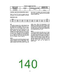
Frequency Divider
The RTC has 22 binary divider stages following
the clock input. The output of the divider is a 1 Hz
signal
to
the
update-cycle
Interrupts
logic. The divider is controlled by the three divider
bits (DV3-DV0) in Register A. As shown in Table
146

 SMSC [ SMSC CORPORATION ]