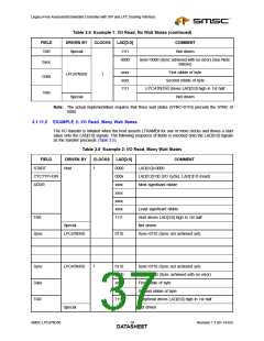
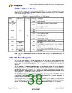
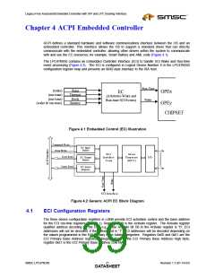
Legacy-Free Keyboard/Embedded Controller with SPI and LPC Docking Interface
Chapter 4 ACPI Embedded Controller
ACPI defines a standard hardware and software communications interface between the OS and an
embedded controller. This interface allows the OS to support a standard driver that can directly
communicate with the embedded controller, allowing other drivers within the system to communicate
with and use the EC resources; for example, Smart Battery and AML code (Figure 4.1).
The LPC47N350 contains an Embedded Controller Interface (ECI) to handle SCI Wake and Run-time
event processing (Figure 4.2). The ECI is configured in Logical Device Number 8 in the LPC47N350
configuration register map and presents an 8042-style interface to the ISA host.
Run-Time
(wake)
(run-time)
Ring
Thermal
Dock
GPEx
GPEy
EC
(Arbitrates Wake and
Run-time SCI Events)
(run-time)
Wake
(wake & run-time)
Battery
Figure 4.1 Embedded Control (EC) Illustration
Command Write
Data Write
Data Read
EC Input
Buffer
SC I
Interface
C ode
M ain
Firmw are
(8051)
EC Output
Buffer
I/O
Status Read
EC Status
Register
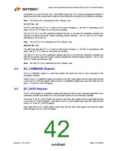
SC I Interface
Figure 4.2 Generic ACPI EC Block Diagram
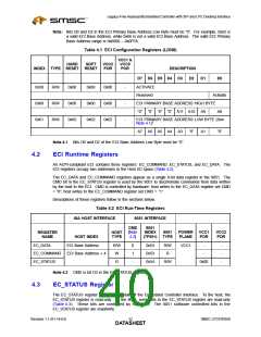
4.1
ECI Configuration Registers
The three device configuration registers in LDN8 provide ECI activation control and the base address
for the ECI run-time registers (Table 4.1). Register 0x30 is the Activate register. The Activate register
qualifies address decoding for the ECI; e.g., if the Activate bit D0 in the Activate register is “0”, ECI
addresses will not be decoded; if the Activate bit is “1”, ECI addresses will be decoded depending on
the values programmed in the ECI Primary Base Address registers. Registers 0x60 and 0x61 are the
ECI Primary Base Address registers. Register 0x60 is the ECI Primary Base Address High Byte,
register 0x61 is the ECI Primary Base Address Low Byte.
SMSC LPC47N350
Revision 1.1 (01-14-03)
DATA2S1HEET

 SMSC [ SMSC CORPORATION ]