Legacy-Free Keyboard/Embedded Controller with SPI and LPC Docking Interface
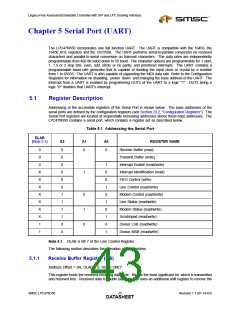
Chapter 5 Serial Port (UART)
The LPC47N350 incorporates one full function UART. The UART is compatible with the 16450, the
16450 ACE registers and the 16C550A. The UART performs serial-to-parallel conversion on received
characters and parallel-to-serial conversion on transmit characters. The data rates are independently
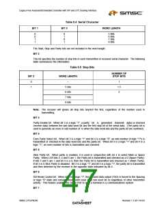
programmable from 460.8K baud down to 50 baud. The character options are programmable for 1 start;
1, 1.5 or 2 stop bits; even, odd, sticky or no parity; and prioritized interrupts. The UART contains a
programmable baud rate generator that is capable of dividing the input clock or crystal by a number
from 1 to 65535. The UART is also capable of supporting the MIDI data rate. Refer to the Configuration
Registers for information on disabling, power down and changing the base address of the UART. The
interrupt from a UART is enabled by programming OUT2 of the UART to a logic "1". OUT2 being a
logic "0" disables that UART's interrupt.
5.1
Register Description
Addressing of the accessible registers of the Serial Port is shown below. The base addresses of the
serial ports are defined by the configuration registers (see Section 23.2, "Configuration Registers"). The
Serial Port registers are located at sequentially increasing addresses above these base addresses. The
LPC47N350 contains a serial port, which contains a register set as described below.
Table 5.1 Addressing the Serial Port
DLAB
(Note 5.1)
A2
A1
A0
REGISTER NAME
Receive Buffer (read)
0
0
0
0
0
0
0
0
1
1
1
1
0
0
0
0
Transmit Buffer (write)
0
1
0
0
1
0
1
0
1
0
1
Interrupt Enable (read/write)
Interrupt Identification (read)
FIFO Control (write)
X
X
X
X
X
X
X
1
1
Line Control (read/write)
Modem Control (read/write)
Line Status (read/write)
Modem Status (read/write)
Scratchpad (read/write)
Divisor LSB (read/write)
Divisor MSB (read/write)
0
1
0
1
Note 5.1 DLAB is Bit 7 of the Line Control Register
The following section describes the operation of the registers.
5.1.1
Receive Buffer Register (RB)
Address Offset = 0H, DLAB = 0, READ ONLY
This register holds the received incoming data byte. Bit 0 is the least significant bit, which is transmitted
and received first. Received data is double buffered; this uses an additional shift register to receive the
SMSC LPC47N350
Revision 1.1 (01-14-03)
DATA2S5HEET

 SMSC [ SMSC CORPORATION ]