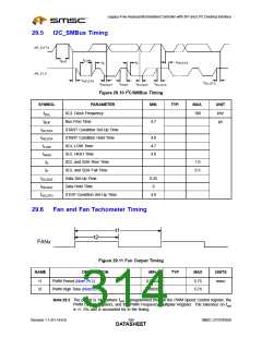
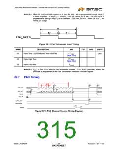
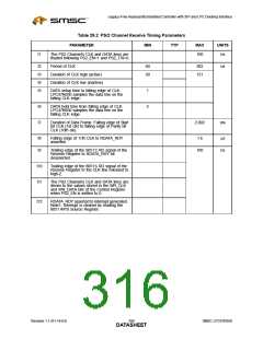
Legacy-Free Keyboard/Embedded Controller with SPI and LPC Docking Interface
Table 29.3 PS/2 Channel Transmission Timing Parameters (continued)
PARAMETER
MIN
TYP
MAX
UNITS
t13
t14
Trailing edge of PS_T/R to XMIT_IDLE bit asserted.
100
ns
DATA released to high-Z following the PS2_T/R bit
going low.
t15
t16
XMIT_IDLE bit driven high to interrupt generated.
Note1- Interrupt is cleared by reading the 8051 INT0
Source Register.
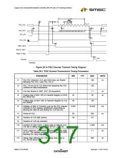
The PS2 Channel’s CLK and DATA lines are driven to
the values stored in the WR_CLK and WR_DATA bits of
the Control Register when PS2_EN is written to 0.
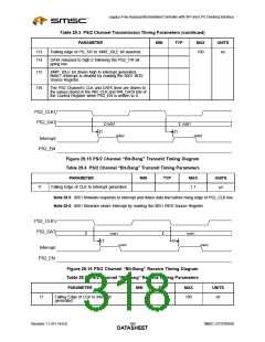
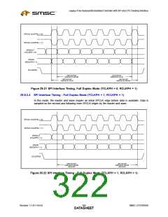
PS2_CLK1
PS2_DAT
note1
note1
t1
t1
note2
note2
Interrupt
PS2_EN
Figure 29.15 PS/2 Channel “Bit-Bang” Transmit Timing Diagram
Table 29.4 PS/2 Channel “Bit-Bang” Transmit Timing Parameters
PARAMETER
Falling Edge of CLK to Interrupt generated.
MIN
TYP
MAX
UNITS
t1
1.1
µs
Note 29.5 8051 firmware responds to interrupt and drives data line before rising edge of PS2_CLK line.
Note 29.6 8051 firmware clears Interrupt by reading the 8051 INT0 Source Register.
PS2_CLK1
PS2_DAT
note1
note1
t1
t1
note2
note2
Interrupt
PS2_EN
Figure 29.16 PS/2 Channel “Bit-Bang” Receive Timing Diagram
Table 29.5 PS/2 Channel “Bit-Bang” Receive Timing Parameters
PARAMETER
MIN
TYP
MAX
UNITS
t1
Falling Edge of CLK to Interrupt
generated.
100
ns
Revision 1.1 (01-14-03)
300
SMSC LPC47N350
DATASHEET

 SMSC [ SMSC CORPORATION ]