Legacy-Free Keyboard/Embedded Controller with SPI and LPC Docking Interface
Note 29.3 When Bit 0 of the PWMx registers is 0, then the duty cycle is programmed through Bits[6:1]
of these registers. If Bits[6:1] = “000000”, then the PWMx pin is low. The duty cycle is
programmable through Bits[6:1] to be between 1.56% and 98.44%. When Bit 0 is 1, the
PWMx pin is high.
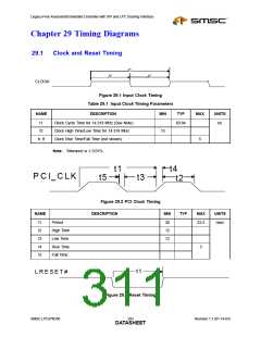
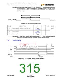
t1
t2
t3
FAN_TACHx
Figure 29.12 Fan Tachometer Input Timing
NAME
DESCRIPTION
MIN
TYP
MAX
UNITS
t1
t2
t3
Pulse Time (1/2 Revolution Time=30/RPM)
4TTACH
µsec
(Note 29.4)
Pulse High Time
3TTACH
(Note 29.4)
Pulse Low Time
TTACH
Note 29.4 tTACH is the clock used for the tachometer counter. It is 30.52* prescaler, where the
prescaler is programmed in the Fan Tachometer Timebase Prescaler register.
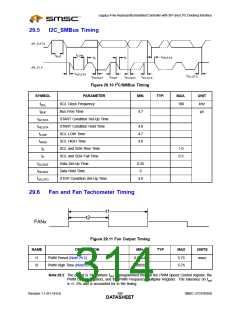
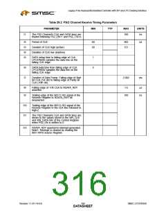
29.7
PS/2 Timing
t7
t3
t5
t10
t11
t2
t4
PS2_CLK
WR_CLK
WR_CLK
t1
t6
PS2_DAT
PS2_EN
PS2_T/R
WR_DATA
b0
b1
b2
b3
b4
b5
b6
b7
P
S
WR_DATA
t8
t9
RDATA_RDY
Read RX Reg
t12
note1
Interrupt
Figure 29.13 PS/2 Channel Receive Timing Diagram
SMSC LPC47N350
297
Revision 1.1 (01-14-03)
DATASHEET

 SMSC [ SMSC CORPORATION ]