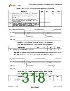
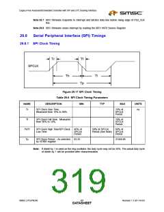
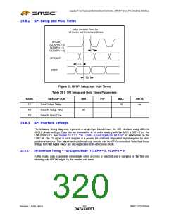
Legacy-Free Keyboard/Embedded Controller with SPI and LPC Docking Interface
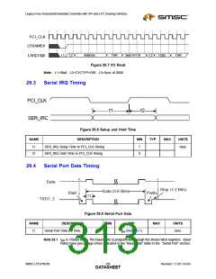
t10
t8
t2
t5
t6
t7
t9
10 11
PS2_CLK
1
2
t1
t4
t11
t14
t16
PS2_DAT
PS2_EN
S
b0 b1 b2 b3 b4 b5 b6 b7
P
t12
PS2_T/R
t3
t13
XMIT_IDLE
RDATA_RDY
Write TX Reg
t15
note1
Interrupt
ORION005
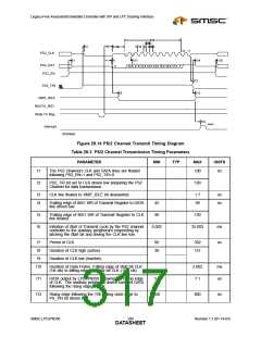
Figure 29.14 PS/2 Channel Transmit Timing Diagram
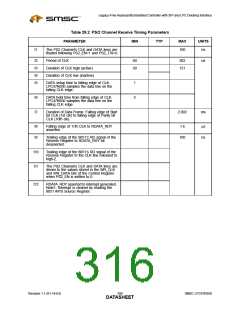
Table 29.3 PS/2 Channel Transmission Timing Parameters
PARAMETER
MIN
TYP
MAX
UNITS
t1
t2
The PS2 Channel’s CLK and DATA lines are floated
following PS2_EN=1 and PS2_T/R=0.
100
ns
PS2_T/R bit set to CLK driven low preparing the PS2
Channel for data transmission.
100
t3
t4
CLK line floated to XMIT_IDLE bit deasserted.
1.7
90
us
ns
Trailing edge of 8051 WR of Transmit Register to DATA
line driven low.
45
90
t5
t6
Trailing edge of 8051 WR of Transmit Register to CLK
line floated.
130
Initiation of Start of Transmit cycle by the PS2 channel
controller to the auxiliary peripheral’s responding by
latching the Start bit and driving the CLK line low.
0.002
25.003
ms
us
t7
t8
Period of CLK
60
30
302
151
Duration of CLK high (active)
Duration of CLK low (inactive)
t9
t10
Duration of Data Frame. Falling edge of Start bit CLK
(1st clk) to falling edge of Parity bit CLK (10th clk).
2.002
7.1
ms
us
t11
t12
DATA output by LPC47N350 following the falling edge
of CLK. The auxiliary peripheral device samples DATA
following the rising edge of CLK.
3.5
Rising edge following the 11th falling clock edge to
PS_T/R bit driven low.
400
800
ns
SMSC LPC47N350
299
Revision 1.1 (01-14-03)
DATASHEET

 SMSC [ SMSC CORPORATION ]