Legacy-Free Keyboard/Embedded Controller with SPI and LPC Docking Interface
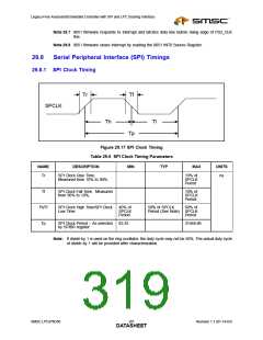
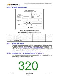
29.8.2 SPI Setup and Hold Times
Setup and Hold Times for
Full-Duplex and Bidrectional Modes
SPCLK
(CLKPOL = 0,
TCLKPH = 0,
RCLKPH = 0)
T1
SPDOUT
T2
SPDIN
T3
Figure 29.18 SPI Setup and Hold Times
Table 29.7 SPI Setup and Hold Times Parameters
NAME
DESCRIPTION
MIN
TYP
MAX
UNITS
T1
T2
T3
Data Output Delay
Data IN Setup Time
Data IN Hold Time
10
ns
20
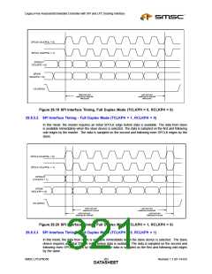
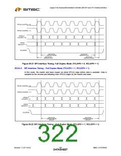
29.8.3 SPI Interface Timings
The following timing diagrams represent a single-byte transfer over the SPI interface using different
SPCLK phase settings. Data bits are transmitted in bit order starting with the MSB (LSBF=‘0’) or the
LSB (LSBF=‘1’). See Section 16.7.1.1, "D0 - LSBF - Least Significant Bit First" for information on the
LSBF bit. The CS signal in each diagram is a generic bit-controlled chip select signal required by most
peripheral devices. This signal and additional chip selects can be GPIO controlled. Note that these
timings for Full Duplex Mode are also applicable to Bi-directional mode.
29.8.3.1 SPI Interface Timing – Full Duplex Mode (TCLKPH = 0, RCLKPH = 0)
In this mode, data is available immediately when a device is selected and is sampled on the first and
following odd SPCLK edges by the master and slave.
Revision 1.1 (01-14-03)
302
SMSC LPC47N350
DATASHEET

 SMSC [ SMSC CORPORATION ]