Legacy-Free Keyboard/Embedded Controller with SPI and LPC Docking Interface
SPCLK (CLKPOL = 0)
SPCLK (CLKPOL = 1)
SPDOUT
(TCLKPH = 0)
SPDIN
(RCLKPH = 0)
CS (GPIO)
FIRST DATA BIT
SAMPLED BY MASTER
AND SLAVE
LAST DATA BIT
SAMPLED BY MASTER
AND SLAVE
Figure 29.19 SPI Interface Timing, Full Duplex Mode (TCLKPH = 0, RCLKPH = 0)
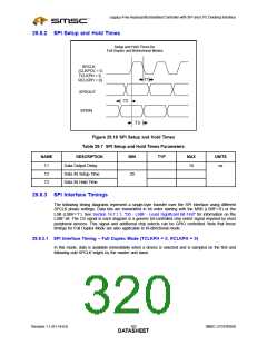
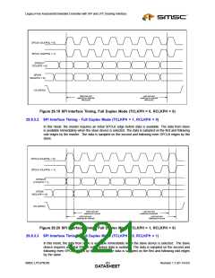
29.8.3.2 SPI Interface Timing - Full Duplex Mode (TCLKPH = 1, RCLKPH = 0)
In this mode, the master requires an initial SPCLK edge before data is available. The data from slave
is available immediately when the slave device is selected. The.data is sampled on the first and following
odd edges by the master. The data is sampled on the second and following even SPCLK edges by the
slave.
SPCLK (CLKPOL = 0)
SPCLK (CLKPOL = 1)
SPDOUT
(TCLKPH = 1)
SPDIN
(RCLKPH = 0)
CS (GPIO)
FIRST DATA BIT
SAMPLED BY SLAVE
LAST DATA BIT
SAMPLED BY MASTER
FIRST DATA BIT
SAMPLED BY MASTER
LAST DATA BIT
SAMPLED BY SLAVE
Figure 29.20 SPI Interface Timing, Full Duplex Mode (TCLKPH = 1, RCLKPH = 0)
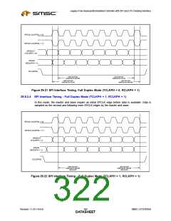
29.8.3.3 SPI Interface Timing - Full Duplex Mode (TCLKPH = 0, RCLKPH = 1)
In this mode, the data from slave is available immediately when the slave device is selected. The slave
device requires an initial SPCLK edge before data is available. The data is sampled on the second and
following even SPCLK edges by the master. The data is sampled on the first and following odd edges
by the slave.
SMSC LPC47N350
303
Revision 1.1 (01-14-03)
DATASHEET

 SMSC [ SMSC CORPORATION ]