Legacy-Free Keyboard/Embedded Controller with SPI and LPC Docking Interface
Note: The 8051 will be reset when exiting KCBM mode if the PGM pin is asserted while the nEA pin
is deasserted.
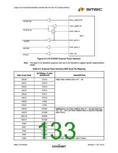
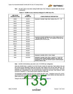
Table 9.7 KCBM Access Interfaces Mapped To KBD Scan Pin
KBD SCAN
KCBM
INTERFACE PINS
INTERFACE
KCBM INTERFACE DESCRIPTION
KSO0
KSO1
KSO2
KSO3
KSO4
KSO5
KSO6
KSO7
KSO8
KSO9
KSO10
KSO11
KSI0
KCA15
KCA14
KCA13
KCA12
KCA11
KCA10
KCA9
Keyboard Controller High-Order Address Bus A15 – A8.
KCA8
KCAD7
KCAD6
KCAD5
KCAD4
KCAD3
KCAD2
KCAD1
KCAD0
KCCLK
KCDSTB
Keyboard Controller Multiplexed Low-Order Address Bus A7
– A0 and Data Bus D0 – D7. The contents of this bus are
indicated by the KCDSTB pin.
KSI1
KSI2
KSI3
KSI4
Keyboard Controller (8051) Clock Output.
KSI5
Keyboard Controller Data Strobe: asserted (‘1’) when the
KCAD[7:0] pins contain program memory code data and
deasserted (‘0’) when the KCAD[7:0] pins contain program
memory address data.
Note: All KDB SCAN Interface pins refer to the LPC47N350 pin configuration.
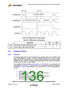
When the KCBM mode is enabled, the KCA[15:8] pins contain the high-order Flash address bits and
the KCAD[7:0] pins alternately contain the low-order Flash address bits and the Flash data bits. The
Keyboard Controller Data Strobe (KCDSTB) determines the contents of the KCAD[7:0] pins. When the
KCDSTB pin is deasserted (‘0’), the KCAD[7:0] pins contain the low-order Flash address, when
KCDSTB is asserted (‘1’), the KCAD[7:0] pins contain the Flash data.
The Keyboard Controller Clock pin (KCCLK) contains the 8051 clock. Transitions on the KCA, KCAD,
and KCDSTB pins occur following the rising edge of KCCLK. The Flash address and data values are
stable before the subsequent rising edge of KCCLK.
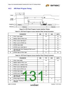
Timing for the KCBM Interface is shown below in Figure 9.8 and Table 9.8.
SMSC LPC47N350
117
Revision 1.1 (01-14-03)
DATASHEET

 SMSC [ SMSC CORPORATION ]