Legacy-Free Keyboard/Embedded Controller with SPI and LPC Docking Interface
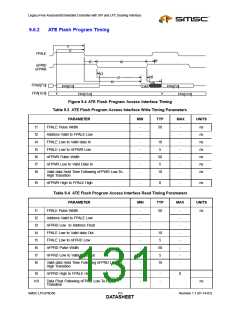
Note: The values in Table 9.3 and Table 9.4 come from SMSC ATE testing.
1
2
3
4
5
6
testvector
00h
80h
validdata
validdata
00h
FFh
validdata
validdata
validaddr
validaddr
FPA15:8
FPAD7:0
FPALE
nFPRD
nFPWR
PGM
providedatatobe
programmedinto
flash
ALElatchesvalid
address
issuea CSI
issueaCSIread
command
readbyvaliddata
formflash
wait48us
progamcommand
y
y
y
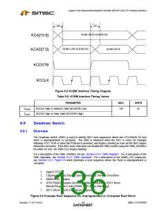
Testcycletimeis60ns.
PulsewidthofFPALE,nFPRD,andnPFWRis50ns.
Thewaitinvector4is1200x60ns=48us
Figure 9.5 ATE Flash Program Access Interface Write Timing Parameters
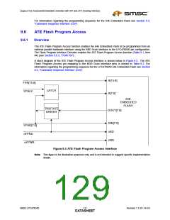
9.6.3
PGM Pin
The PGM pin enables the ATE Flash Program access function. When the PGM pin is the exclusively
asserted input to the Flash Program Interface Decoder (Table 9.1, item #4), the 64k Embedded Flash
interface is directly connected to the ATE Flash Program Access interface, the KBD Scan interface pin
multiplexing is configured to support ATE Flash Program Access, the 8051 is stopped (reset), and all
Flash write-protect functions are disabled (see Section 8.5, "8051 Flash Boot Block Protect Controls").
To stop the 8051, the PGM pin asserting (‘1’) causes the rst_in_n input to the 8051 is asserted (‘0’).
When the PGM pin is deasserted, the 64k Embedded Flash interface is reconnected to the 8051, the
Embedded Flash is reset to READ ARRAY mode, the rst_in_n input to the 8051 is deasserted and the
Flash write-protect function is re-enabled.
9.7
External Flash Interface
The External Flash Interface function enables the 8051 program memory to reside in an external ROM
device using the KBD Scan Interface in the LPC47N350 pin configuration.
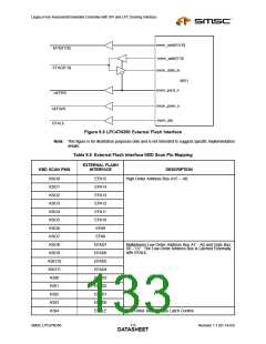
A block diagram of the External Flash Interface is shown below in Figure 9.6. The External Flash
Interface pin mapping to the KBD Scan interface pins is shown in Table 9.5. The Flash Program
Interface Decoder enables the the External Flash Interface function (Table 9.1, item #5). When the nEA
pin is asserted, the 8051 program memory is disconnected from 64k Embedded Flash interface and
connected to the External Flash Interface, the KBD Scan interface pin multiplexing is configured to
support the External Flash Interface, and the 64k Embedded Flash is placed in a Reset state (see
Section 8.3.3, "Reset," on page 90).
Note: The LPC47N350 External Flash Interface only supports 8051 ROM read cycles (Figure 9.7 and
Table 9.6). The External Flash Interface is compatible with flash devices like the Intel 28F004.
The 8051 normally uses the mem_wr_n signal as a write strobe for its data RAM. Optionally, it can
perform writes to code ROM using the mem_pswr_n signal. When the WRS Control bit D0 is set to “1”
in the SPC_FNC SFR (See Section 8.3.5, "CSI Command Types"), the DW8051 uses the mem_pswr_n
signal instead of the mem_wr_n when MOVX instructions are executed. By attaching mem_pswr_n to
its 64K code space, the 8051 can perform writes to its code space when the WRS bit is set to “1”.
Revision 1.1 (01-14-03)
114
SMSC LPC47N350
DATASHEET

 SMSC [ SMSC CORPORATION ]