Legacy-Free Keyboard/Embedded Controller with SPI and LPC Docking Interface
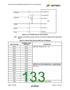
Table 9.5 External Flash Interface KBD Scan Pin Mapping (continued)
EXTERNAL FLASH
KBD SCAN PINS
INTERFACE
DESCRIPTION
KSI5
KSI6
nEFRD
nEFWR
Active-Low External Flash Interface READ Signal.
Active-Low External Flash Interface WRITE Signal.
Note: All External Flash Interface signals in Table 9.5 refer to Figure 9.6. All KDB SCAN Interface pins
refer to the LPC47N350 pin configuration.
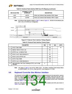
t1
t2
EFALE
nEFR D
t5
t6
t3
t7
t8
t9
t4
EFAD [7:0]
EFA[15:8]
EFA[7:0]
IN S
EF A[7:0]
EFA[15:8]
EFA[15:8]
Figure 9.7 External Flash Interface Timing Diagram
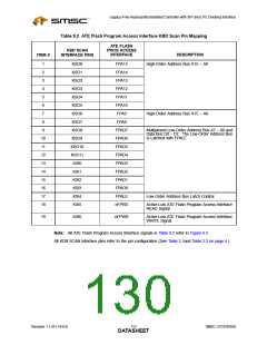
Table 9.6 External Flash Interface Timing Values
PARAMETER
MIN
TYP
MAX
UNITS
t1
t2
t3
t4
t5
t6
t7
t8
EFALE Pulse Width
Address Valid to EFALE Low
125
86
ns
nEFRD Low to Address Float
EFALE Low to Valid Instruction In
EFALE Low to nEFRD Low
nEFRD Pulse Width
5
83
160
160
145
nEFRD Low to Valid Instruction In
Valid Instruction Hold Time Following nEFRD Low-To-High
Transition
0
Note: The values in Table 9.6 are for the 12MHz Clock. The SMSC evaluation board design utilizes
an AM29F002NBT-120 (120 ns ) flash and 8051 clock frequency of 12 MHz
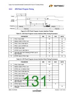
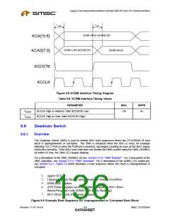
9.8
Keyboard Controller Bus Monitor Interface
The Keyboard Controller Bus Monitor (KCBM) functions provide monitoring for the internal 8051 memory
ROM bus using the KBD Scan interface pins. When the KCBM is enabled, reads from the 8051 code
space are visible on the KCBM interface pins. The three KCBM functions provide external access
modes corresponding to 8051 CODE FETCH ACCESS, LPC PROGRAM ACCESS, 8051 PROGRAM
ACCESS (Table 9.1, items #6, 7 and 8)
When the PGM and nEA pins are asserted, the KCBM interface is enabled and all the pins shown in
Table 9.2 are outputs.
Revision 1.1 (01-14-03)
116
SMSC LPC47N350
DATASHEET

 SMSC [ SMSC CORPORATION ]