LC89057W-VF4A-E
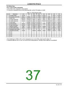
12.2 Write Data
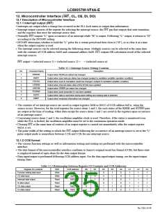
12.2.1 List of write commands
•
A list of the write commands is shown below.
•
To write the commands shown in the following table, set the CCB address to 0xE8.
Table 12.3 Write Register Map
Add.
0
Setting Items
All system setting
Demodulation system setting
Master clock
DI15
TESTM
PBSEL1
AMPOPR1
XRLRCK1
XSLRCK1
0
DI14
DI13
TXOPR
FSLIM1
EXSYNC
XRBCK1
XSBCK1
RDTSTA
ROSEL1
RLRCKP
PCRNW
FSERR
P11
DI12
RXOPR
FSLIM0
PLLOPR
XRBCK0
XSBCK0
RDTSEL
ROSEL0
RBCKP
UNPCM
RESTA
P10
DI11
DI10
0
DI9
DOEN
VOSEL
XINSEL
PRSEL1
PSBCK1
OCKSEL
RISEL1
OFSEL1
INDET
REDER
VISEL
TWLRP
0
DI8
SYSRST
UOSEL
PLLSEL
PRSEL0
PSBCK0
SELMTD
RISEL0
OFSEL0
ERROR
RESEL
UISEL
TXDFS
0
0
INTOPF
1
PBSEL0
AMPOPR0
XRLRCK0
XSLRCK0
RDTMUT
ROSEL2
SBCKP
SLIPO
ERWT0
P12
RXMON
AOSEL
XMSEL0
XRSEL0
PSLRCK0
RCKSEL
RISEL2
OFSEL2
FSCHG
XTWT0
VMODE
TDTSEL
0
2
XMSEL1
3
R system output clock
S system output clock
Source switch
XRSEL1
4
PSLRCK1
5
0
6
Data input/output
RXOFF
SLRCKP
EMPF
ERWT1
P13
ULSEL
7
Output format setting
___
INTsource selection
0
8
CSRNW
9
RERR condition setting
XTWT1
10
11
12
13
14
15
Modulation system setting
0
Modulation data setting
TCKSEL
0
0
TXMOD1
0
TXMOD0
0
TXMUT
TEST
TEST
TEST
TEST
0
0
0
0
0
0
0
0
0
0
0
0
0
0
0
0
0
0
0
0
0
0
0
0
0
0
•
•
The shaded parts of DI8 to DI15 in the command area are reserved bits. Input must be doing "0".
Command addresses 0x12 to 0x15 are reserved for testing purposes. Writing to these addresses is prohibited.
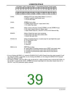
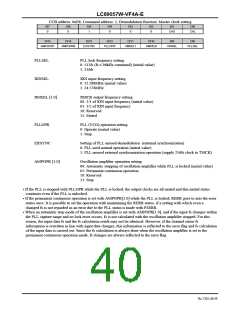
No.7202-37/59

 SANYO [ SANYO SEMICON DEVICE ]