LC89057W-VF4A-E
11.1.5 Modulated output of SDIN input data
•
•
•
•
SDIN input data is modulated and its output can be fetched from TXO and RXOUT.
To modulate SDIN input data, set it with TDTSEL.
Input a clock synchronized with SDIN to TMCK, TBCK, and TLRCK.
The SDIN input data format must be identical to the setting used during modulation processing.
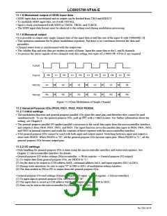
11.1.6 Monaural output
•
It is possible to output only single channel data of the input data at half the rate of the input fs with TXMOD[1:0].
•
This operation maintains the bi-phase modulation regularity, but there is no correlation between the data and
preambles.
•
Channel status write is synchronized with the output rate.
•
The validity flag and user data are written in units of frame. Input the same data to the L and R channels.
•
To process the stereo signals of two channels with this setting, two units of LC89057W-VF4A-E are required.
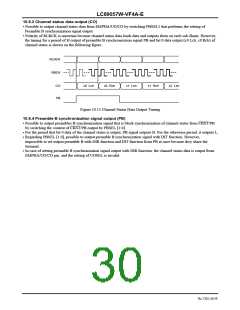
TLRCK
R0
L1
R1
L2
R2
L3
R3
L4
R4
L5
R5
TDATA
TXO [1]
TXO [2]
Ln
M
L0
W
L1
M
L2
W
L3
M
L4
Rn
M
R0
W
R1
M
R2
W
R3
M
R4
Figure 11.4 Data Modulation of Single Channel
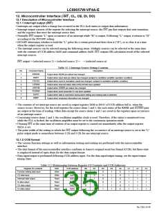
11.2 General-Purpose I/Os (PIO0, PIO1, PIO2, PIO3 PIOEN)
11.2.1 Initial settings
•
The modulation function and general-purpose parallel I/Os share the same pins and therefore they cannot be used
______
simultaneously. To use the general-purpose I/Os, pull up INT with a 10kΩ resistor. For further information about the
setting, see Chapter 9.
•
•
The general-purpose parallel I/O applies parallel-conversion to the serial data input from the microcontroller interface,
and outputs it from PIO0, PIO1, PIO2, and PIO3. The input function saves the parallel data input to PIO0, PIO1, PIO2,
and PIO3 in internal registers and reads the contents of these registers with the microcontroller interface.
4-bit general-purpose I/Os cannot be used with both input and output mixed. Switching between input and output is
done with PIOEN. When PIOEN is "H", all the general-purpose I/Os become input pins. When PIOEN is "L", all the
general-purpose I/Os become output pins.
11.2.2 I/O settings
•
Data handling for general-purpose I/Os is done using the microcontroller interface and write/read registers. See
Chapter 12 Microcontroller Interface for details.
•
General-purpose I/O writes settings (Microcontroller → Write register → General-purpose I/O output)
(1) To output data from general-purpose I/Os, set PIOEN to "L".
(2) Set the data to be output to CCB address 0xE8, command address 0x10, and input registers DI12 to DI15.
(3) During write operation, be sure to input "0" to DI8 to DI11 of modulation setting registers.
(4) The data written to PI0 to PI3 is output from the general-purpose I/Os.
•
General-purpose I/O read settings (General-purpose I/O input → Read register → Microcontroller)
(1) To input data to general-purpose I/Os, set PIOEN to "H".
(2) The input data is saved in CCB address 0xEB and output registers DO0 to DO3.
(3) Data can be sent to the microcontroller by reading PO0 to PO3.
No.7202-34/59

 SANYO [ SANYO SEMICON DEVICE ]