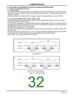
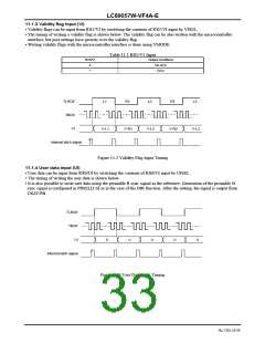
LC89057W-VF4A-E
12.1.3 Data write procedure
•
Input is performed in the following sequence: CCB addresses of A0 to A3 and B0 to B3, chip addresses of DI0 and
DI1, command addresses of DI4 to DI7, and data of DI8 to DI15. DI2 and DI3 are reserved for the system. Input must
be doing "0".
•
For the chip addresses, DI0 corresponds to CAL (low-order), and DI1 to CAU (high-order). For details, see section 9.2.
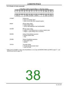
12.1.4 Data read procedure
•
Read data is output from DO. DO is in the high impedance state when CE is "L", and begins outputting from the rising
edge of CE after output setting is established at the CCB address. DO then returns to the high impedance state at the
falling edge of CE.
•
If DO outputs are shared using multiple LC89057W-VF4A-E units, it is possible to set the DO outputs of the
LC89057W-VF4A-E units of which data is not to be read to be always in the high impedance state with DOEN. With
this setting, only the targeted outputs can be read.
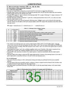
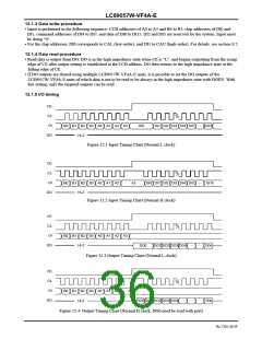
12.1.5 I/O timing
CE
CL
…
DI15
DI
B0 B1 B2 B3 A0 A1 A2 A3
Hi-Z
DI0
DI1 DI2 DI3 DI4 DI5
DO
Figure 12.1 Input Timing Chart (Normal L clock)
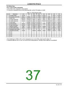
CE
CL
DI
…
B0 B1 B2 B3 A0 A1 A2
Hi-Z
A3
DI0 DI1 DI2 DI3 DI4 DI5
DI15
DO
Figure 12.2 Input Timing Chart (Normal H clock)
CE
CL
DI
B0 B1 B2 B3 A0 A1 A2 A3
Hi-Z
…
…
DO
DO0
DO1 DO2 DO3 DO4
DOn
Figure 12.3 Output Timing Chart (Normal L clock)
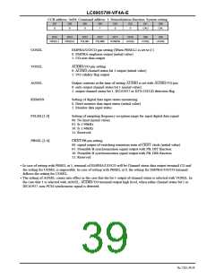
CE
CL
DI
B0 B1 B2 B3 A0 A1 A2
Hi-Z
A3
…
…
…
DO
DO0 DO1 DO2 DO3 DO4
DOn
Figure 12.4 Output Timing Chart (Normal H clock, DO0 need be read with port)
No.7202-36/59

 SANYO [ SANYO SEMICON DEVICE ]