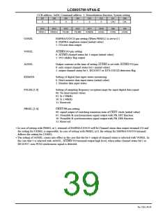
LC89057W-VF4A-E
12.2.2 Details of write commands
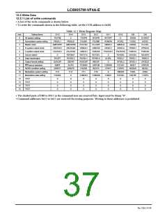
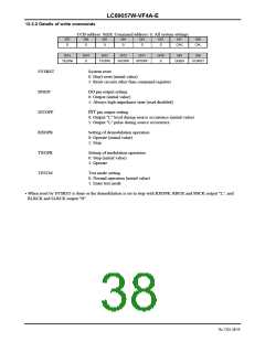
CCB address: 0xE8; Command address: 0; All system settings
DI7
0
DI6
0
DI5
0
DI4
0
DI3
0
DI2
0
DI1
DI0
CAU
CAL
DI15
DI14
0
DI13
DI12
DI11
DI10
0
DI9
DI8
TESTM
TXOPR
RXOPR
INTOPF
DOEN
SYSRST
SYSRST
DOEN
System reset
0: Don't reset (initial value)
1: Reset circuits other than command registers
DO pin output setting
0: Output (initial value)
1: Always high impedance state (read disabled)
______
INTOPF
RXOPR
TXOPR
TESTM
INT pin output setting
0: Output "L" level during source occurrence (initial value)
1: Output "L" pulse during source occurrence
Setting of demodulation operation
0: Operate (initial value)
1: Stop
Setting of modulation operation
0: Stop (initial value)
1: Operate
Test mode setting
0: Normal operation (initial value)
1: Enter test mode
•
When reset by SYSRST is done or the demodulation is set to stop with RXOPR, RBCK and SBCK output "L", and
RLRCK and SLRCK output "H".
No.7202-38/59

 SANYO [ SANYO SEMICON DEVICE ]