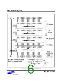
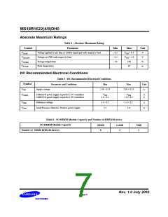
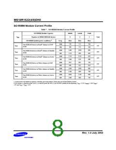
MS18R1622(4/8)DH0
AC Electrical Specifications
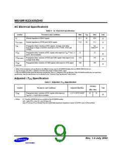
Table 8 : AC Electrical Specifications
Parameter and Conditions
Module Impedance of RSL Signals
Symbol
ZL
ZUL-CMOS
TPD
Min
Typ
Max
Unit
Ω
25.2
28
30.8
Module Impedance of SCK and CMOS signals
23.8
-
28
32.2
Ω
Propagation Delay variation of RSL signals. Average clock delay
from finger to finger of all RSL clock nets (CTM, CTMN, CFM, and
CFMN)
See
Table10a,b
ns
∆TPD
Propagation delay variation of RSL signals with respect to TPD b,c for 2, 4
and 8 device modules
-21
-250
-200
21
ps
ps
ps
∆TPD-CMOS
Propagation delay variation of SCK and CMD signals with respect to an
average clock delay
250
200
∆TPD-
Propagation delay variation of CMD signals with respect to SCK signal
SCK,CMD
a. Table 10 lists parameters and specifications for different storage capacity SO-RIMM Modules that use 288Mb RDRAM devices.
b. T or Average clock delay is defined as the delay from finger to finger of RSL signal.
PD
c. If the SO-RIMM module meets the following specification, then it is compliant to the specification. If the SO-RIMM module does not meet these
specifications, then the specification can be adjusted by the “Adjusted ∆T Specification“ table 9 below.
PD
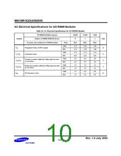
Adjusted ∆TPD Specification
Table 9 : Adjusted ∆TPD Specification
Absolute
Symbol
Parameter and Conditions
Adjusted Min/Max
Unit
Min / Max
∆TPD
Propagation delay variation of RSL signals with respect to
+/-[17+(18*N*∆Z0)]a
-30
30
ps
TPD for 2, 4 and 8 device modules
a. Where:
N = Number of RDRAM devices installed on the SO-RIMM module
∆Z0 = delta Z0% = (max Z0 - min Z0)/(min Z0)
(max Z0 and min Z0 are obtained from the loaded (high impedance) impedance coupons of all RSL layers on the modules)
Rev. 1.0 July 2002
Page 8

 SAMSUNG [ SAMSUNG ]