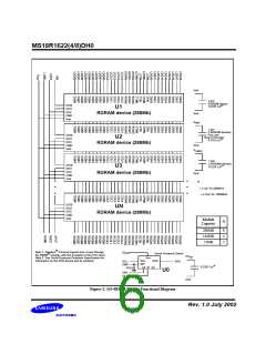
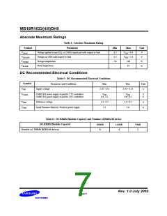
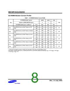
MS18R1622(4/8)DH0
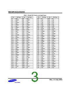
Signal
Pins
I/O
I
Type
RSL
Description
Clock to master. Interface clock used for transmitting RSL
signals to the Channel. Positive polarity.
RCTM
B69
B67
Clock to master. Interface clock used for transmitting RSL
signals to the Channel. Negative polarity.
RCTMN
I
RSL
RSL
Data bus A. A 9-bit bus carrying a byte of read or write data
between the Channel and the RDRAM device. RDQA8 is
non-functional on modules x16 RDRAM devices.
RDQA8..
RDQA0
B79, A79, B77, A77, B75, A75, B73,
A73, B71
I/O
Data bus B. A 9-bit bus carrying a byte of read or write data
between the Channel and the RDRAM device. RDQB8 is
non-functional on modules x16 RDRAM devices.
RDQB8..
RDQB0
A51, A53, B51, A55, B53, A57, B55,
A59, B57
I/O
RSL
RROW2..
RROW0
Row bus. 3-bit bus containing control and address information
for row accesses.
A67, B65, A65
A49
I
I
RSL
Serial Clock input. Clock source used to read from and write
to the RDRAM control registers.
RSCK
VCMOS
SA0
SA1
SCL
SDA
B43
B45
A43
A45
I
I
SVDD
SVDD
SVDD
SVDD
Serial Presence Detect Address 0.
Serial Presence Detect Address 1.
Serial Presence Detect Clock.
I
I/O
Serial Presence Detect Data (Open Collector I/O).
Serial I/O. Pin for reading from and writing to the control reg-
SIN
B34
A34
I/O VCMOS isters. Attaches to SIO0 of the first RDRAM device on the
module.
Serial I/O. Pin for reading from and writing to the control reg-
I/O VCMOS isters. Attaches to SIO1 of the last RDRAM device on the
module.
SOUT
SPD Voltage. Used for signals SCL, SDA, SWE, SA0, SA1
and SA2.
SVDD
SWP
A47
B47
Serial Presence Detect Write Protect (active high). When low,
the SPD can be written as well as read.
I
SVDD
VCMOS
Vdd
A39, B39
CMOS I/O Voltage. Used for signals CMD, SCK, SIN, SOUT.
A35, B35, A44, B44, A46, B46
A42, B42
Supply voltage for the RDRAM core and interface logic.
Logic threshold reference voltage for RSL signals.
Vref
Rev. 1.0 July 2002
Page 4

 SAMSUNG [ SAMSUNG ]