K7I163682B
K7I161882B
512Kx36 & 1Mx18 DDRII CIO b2 SRAM
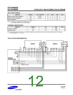
PIN CAPACITANCE
PRMETER
Address Control Input Capacitance
Input and Output Capacitance
Clock Capacitance
SYMBOL
CIN
TESTCONDITION
TYP
MAX
UNIT
pF
NOTE
VIN=0V
VOUT=0V
-
4
6
5
5
7
6
COUT
pF
CCLK
pF
Note: 1. Parameters are tested with RQ=250Ω and VDDQ=1.5V.
2. Periodically sampled and not 100% tested.
THERMAL RESISTANCE
PRMETER
Junction to Ambient
Junction to Case
SYMBOL
TYP
17.1
3.3
UNIT
NOTE
θJA
θJC
°C/W
°C/W
Note: Junction temperature is a function of on-chip power dissipation, package thermal impedance, mounting site temperature and mounting site
thermal impedance. TJ=TA + PD x θJA
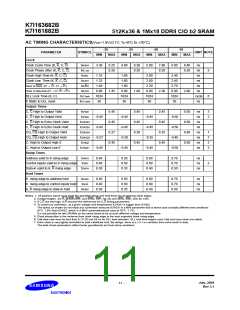
APPLICATION INRORMATION
R=250Ω
R=250Ω
ZQ
ZQ
ZQ
SRAM#1
SRAM#4
CQ
CQ
Q
CQ
CQ
Q
Vt
D
D
SA
SA
R W BW0 BW1 C C K K
RW BW0 BW1 C C K K
R
Data In
Data Out
Address
R
Vt
Vt
R
W
BW
MEMORY
CONTROLLER
Return CLK
Vt
Vt
Source CLK
Return CLK
Source CLK
R=50Ω Vt=VREF
SRAM1 Input CQ
SRAM1 Input CQ
SRAM4 Input CQ
SRAM4 Input CQ
July. 2004
Rev 3.1
- 12 -

 SAMSUNG [ SAMSUNG ]