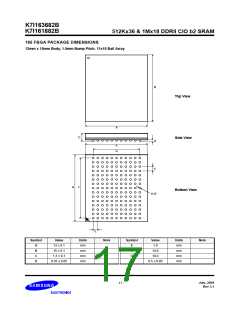
K7I163682B
K7I161882B
512Kx36 & 1Mx18 DDRII CIO b2 SRAM
IEEE 1149.1 TEST ACCESS PORT AND BOUNDARY SCAN-JTAG
This part contains an IEEE standard 1149.1 Compatible Test Access Port(TAP). The package pads are monitored by the Serial Scan
circuitry when in test mode. This is to support connectivity testing during manufacturing and system diagnostics. Internal data is not
driven out of the SRAM under JTAG control. In conformance with IEEE 1149.1, the SRAM contains a TAP controller, Instruction Reg-
ister, Bypass Register and ID register. The TAP controller has a standard 16-state machine that resets internally upon power-up,
therefore, TRST signal is not required. It is possible to use this device without utilizing the TAP. To disable the TAP controller without
interfacing with normal operation of the SRAM, TCK must be tied to VSS to preclude mid level input. TMS and TDI are designed so an
undriven input will produce a response identical to the application of a logic 1, and may be left unconnected. But they may also be
tied to VDD through a resistor. TDO should be left unconnected.
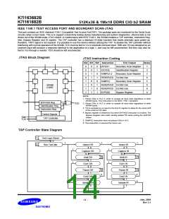
JTAG Block Diagram
JTAG Instruction Coding
IR2 IR1 IR0 Instruction
TDO Output
Notes
0
0
0
1
1
0
0
1
1
0
1
0
1
0
1
0
1
EXTEST
IDCODE
SAMPLE-Z
Boundary Scan Register
Identification Register
Boundary Scan Register
1
3
2
6
5
6
6
4
0
0
0
RESERVED Do Not Use
1
SAMPLE
Boundary Scan Register
1
RESERVED Do Not Use
RESERVED Do Not Use
SRAM
CORE
1
1
BYPASS
Bypass Register
NOTE :
1. Places DQs in Hi-Z in order to sample all input data regardless of other
SRAM inputs. This instruction is not IEEE 1149.1 compliant.
2. Places DQs in Hi-Z in order to sample all input data regardless of other
SRAM inputs.
TDI
BYPASS Reg.
Identification Reg.
Instruction Reg.
TDO
3. TDI is sampled as an input to the first ID register to allow for the serial shift
of the external TDI data.
4. Bypass register is initiated to VSS when BYPASS instruction is invoked. The
Bypass Register also holds serially loaded TDI when exiting the Shift DR
states.
5. SAMPLE instruction dose not places DQs in Hi-Z.
6. This instruction is reserved for future use.
Control Signals
TAP Controller
TMS
TCK
TAP Controller State Diagram
1
0
Test Logic Reset
0
1
1
0
1
Run Test Idle
Select DR
0
Capture DR
0
Shift DR
1
Exit1 DR
0
Select IR
0
1
1
1
1
Capture IR
0
0
Shift IR
1
Exit1 IR
0
0
0
0
0
Pause DR
1
Pause IR
1
Exit2 IR
1
Exit2 DR
1
1
0
Update DR
0
Update IR
1
July. 2004
Rev 3.1
- 14 -

 SAMSUNG [ SAMSUNG ]