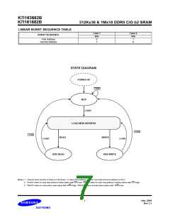
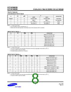
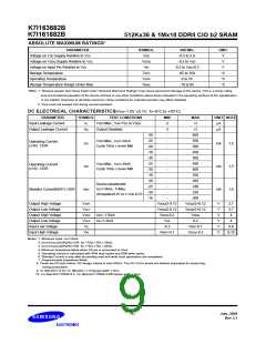
K7I163682B
K7I161882B
512Kx36 & 1Mx18 DDRII CIO b2 SRAM
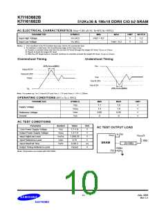
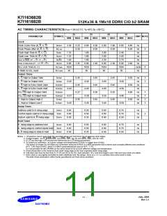
AC TIMING CHARACTERISTICS(VDD=1.8V 0.1V, TA=0°C to +70°C)
-30
-25
-20
-16
PARAMETER
SYMBOL
UNIT NOTE
MIN
MAX
MIN
MAX
MIN
MAX
MIN
MAX
Clock
Clock Cycle Time (K, K, C, C)
Clock Phase Jitter (K, K, C, C)
Clock High Time (K, K, C, C)
Clock Low Time (K, K, C, C)
Clock to Clock (K↑ → K↑, C↑ → C↑)
Clock to data clock (K↑ → C↑, K↑→ C↑)
DLL Lock Time (K, C)
tKHKH
tKC var
tKHKL
3.30
5.25
0.20
4.00
6.30
0.20
5.00
7.88
0.20
6.00
8.40
0.20
ns
ns
ns
5
6
1.32
1.32
1.49
0.00
1024
30
1.60
1.60
1.80
0.00
1024
30
2.00
2.00
2.20
0.00
1024
30
2.40
2.40
2.70
0.00
1024
30
tKLKH
ns
tKHKH
tKHCH
tKC lock
tKC reset
ns
1.45
1.80
2.30
2.80
ns
cycle
ns
K Static to DLL reset
Output Times
C, C High to Output Valid
C, C High to Output Hold
C, C High to Echo Clock Valid
C, C High to Echo Clock Hold
CQ, CQ High to Output Valid
CQ, CQ High to Output Hold
C, High to Output High-Z
C, High to Output Low-Z
Setup Times
tCHQV
tCHQX
0.45
0.45
0.27
0.45
0.45
0.45
0.30
0.45
0.45
0.45
0.35
0.45
0.50
0.50
0.40
0.50
ns
ns
ns
ns
ns
ns
ns
ns
3
3
-0.45
-0.45
-0.27
-0.45
-0.45
-0.45
-0.30
-0.45
-0.45
-0.45
-0.35
-0.45
-0.50
-0.50
-0.40
-0.50
tCHCQV
tCHCQX
tCQHQV
tCQHQX
tCHQZ
7
7
3
3
tCHQX1
Address valid to K rising edge
Control inputs valid to K rising edge
Data-in valid to K, K rising edge
Hold Times
tAVKH
tIVKH
0.40
0.40
0.30
0.50
0.50
0.35
0.60
0.60
0.40
0.70
0.70
0.50
ns
ns
ns
2
tDVKH
K rising edge to address hold
K rising edge to control inputs hold
K, K rising edge to data-in hold
tKHAX
tKHIX
0.40
0.40
0.30
0.50
0.50
0.35
0.60
0.60
0.40
0.70
0.70
0.50
ns
ns
ns
tKHDX
Notes: 1. All address inputs must meet the specified setup and hold times for all latching clock edges.
2. Control singles are R, W,BW0,BW1 and (NW0, NW1, for x8) and (BW2, BW3, also for x36)
3. If C,C are tied high, K,K become the references for C,C timing parameters.
4. To avoid bus contention, at a given voltage and temperature tCHQX1 is bigger than tCHQZ.
The specs as shown do not imply bus contention beacuse tCHQX1 is a MIN parameter that is worst case at totally different test conditions
(0°C, 1.9V) than tCHQZ, which is a MAX parameter(worst case at 70°C, 1.7V)
It is not possible for two SRAMs on the same board to be at such different voltage and temperature.
5. Clock phase jitter is the variance from clock rising edge to the next expected clock rising edge.
6. Vdd slew rate must be less than 0.1V DC per 50 ns for DLL lock retention. DLL lock time begins once Vdd and input clock are stable.
7. Echo clock is very tightly controlled to data valid/data hold. By design, there is a 0.1 ns variation from echo clock to data.
The data sheet parameters reflect tester guardbands and test setup variations.
July. 2004
Rev 3.1
- 11 -

 SAMSUNG [ SAMSUNG ]