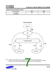
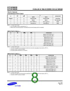
K7I163682B
K7I161882B
512Kx36 & 1Mx18 DDRII CIO b2 SRAM
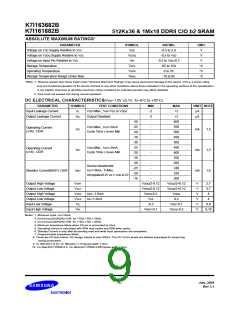
AC ELECTRICAL CHARACTERISTICS (VDD=1.8V 0.1V, TA=0°C to +70°C)
PARAMETER
Input High Voltage
Input Low Voltage
SYMBOL
VIH (AC)
VIL (AC)
MIN
MAX
-
UNIT
V
NOTES
1,2
VREF + 0.2
-
VREF - 0.2
V
1,2
Notes: 1. This condition is for AC function test only, not for AC parameter test.
2. To maintain a valid level, the transitioning edge of the input must :
a) Sustain a constant slew rate from the current AC level through the target AC level, VIL(AC) or VIH(AC)
b) Reach at least the target AC level
c) After the AC target level is reached, continue to maintain at least the target DC level, VIL(DC) or VIH(DC)
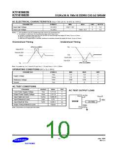
Overershoot Timing
Undershoot Timing
20% tKHKH(MIN)
VIH
VDDQ+0.5V
VDDQ+0.25V
VDDQ
VSS
VSS-0.25V
VSS-0.5V
20% tKHKH(MIN)
VIL
Note: For power-up, VIH ≤ VDDQ+0.3V and VDD ≤ 1.7V and VDDQ ≤ 1.4V t ≤ 200ms
OPERATING CONDITIONS (0°C ≤ TA ≤ 70°C)
PARAMETER
SYMBOL
VDD
MIN
1.7
1.4
0.68
0
MAX
1.9
1.9
0.95
0
UNIT
V
V
V
V
Supply Voltage
VDDQ
VREF
Reference Voltage
Ground
VSS
AC TEST CONDITIONS
Parameter
Symbol
VDD
Value
1.7~1.9
1.4~1.9
1.25/0.25
0.75
Unit
V
AC TEST OUTPUT LOAD
Core Power Supply Voltage
Output Power Supply Voltage
Input High/Low Level
VDDQ
V
0.75V
VREF
VDDQ/2
VIH/VIL
VREF
V
Input Reference Level
V
50Ω
SRAM
Zo=50Ω
Input Rise/Fall Time
TR/TF
0.3/0.3
VDDQ/2
ns
V
Output Timing Reference Level
250Ω
ZQ
Note: Parameters are tested with RQ=250Ω
July. 2004
Rev 3.1
- 10 -

 SAMSUNG [ SAMSUNG ]