K7I163682B
K7I161882B
512Kx36 & 1Mx18 DDRII CIO b2 SRAM
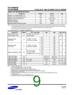
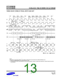
TIMING WAVE FORMS OF READ, WRITE AND NOP
NOP
READ
READ
READ
READ
NOP
NOP
WRITE
WRITE
READ
NOP
NOP
(burst of 2) (burst of 2) (burst of 2)
(burst of 2) (burst of 2) (burst of 2) (burst of 2)
(Note3)
9
5
1
2
4
6
7
8
10
12
3
11
K
K
t
KHKL
t
KHKH
tKHKH
tKLKH
tIVKH
tKHIX
LD
R/W
SA
A2
A5
A6
A0
A1
A3
A4
tKHDX
tDVKH
DQ
Q01
Q02
Q11
Q12
Q21
Q22
D31
D32
D41
D42
Q51
Q52
Q61
Q62
tCHQV
tCHQX
tCHQZ
tCHQV
t
tKKHHKKLH
tKLKH
tKHCH
tCHQX1
C
C
tCHCQX
t
CHCQX
tKHKH
tCHCQV
CQ
CQ
tCHCQV
DON′T CARE
UNDEFINED
NOTE
1. Q01 refers to output from address A. Q02 refers to output from the next internal burst address following A, etc.
2. Outputs are disabled(High-Z) one clock cycle after a NOP .
3. The second NOP cycle is not necessary for correct device operation; however, at high clock frequencies, it may be required to prevent
bus contention.
July. 2004
Rev 3.1
- 13 -

 SAMSUNG [ SAMSUNG ]