K7I163682B
K7I161882B
ABSOLUTE MAXIMUM RATINGS*
512Kx36 & 1Mx18 DDRII CIO b2 SRAM
PARAMETER
Voltage on VDD Supply Relative to VSS
Voltage on VDDQ Supply Relative to VSS
Voltage on Input Pin Relative to VSS
Storage Temperature
SYMBOL
VDD
RATING
-0.5 to 2.9
-0.5 to VDD
-0.5 to VDD+0.3
-65 to 150
0 to 70
UNIT
V
VDDQ
VIN
V
V
TSTG
TOPR
TBIAS
°C
°C
°C
Operating Temperature
Storage Temperature Range Under Bias
-10 to 85
*Note: 1. Stresses greater than those listed under "Absolute Maximum Ratings" may cause permanent damage to the device. This is a stress rating
only and functional operation of the device at these or any other conditions above those indicated in the operating sections of this specification
is not implied. Exposure to absolute maximum rating conditions for extended periods may affect reliability.
2. VDDQ must not exceed VDD during normal operation.
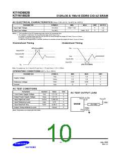
DC ELECTRICAL CHARACTERISTICS(VDD=1.8V 0.1V, TA=0°C to +70°C)
PARAMETER
Input Leakage Current
Output Leakage Current
SYMBOL
TEST CONDITIONS
VDD=Max ; VIN=VSS to VDDQ
Output Disabled,
MIN
MAX
+2
UNIT NOTE
IIL
-2
-2
-
µA
µA
IOL
+2
-30
-25
-20
-16
-30
-25
-20
-16
-30
-25
-20
-16
600
-
550
VDD=Max , IOUT=0mA
Cycle Time ≥ tKHKH Min
Operating Current
(x36) : DDR
ICC
ICC
mA
mA
mA
1,5
1,5
1,6
-
500
450
-
-
-
500
450
VDD=Max , IOUT=0mA
Cycle Time ≥ tKHKH Min
Operating Current
(x18) : DDR
400
350
-
260
Device deselected,
IOUT=0mA, f=Max,
All Inputs≤0.2V or ≥ VDD-0.2V
-
240
Standby Current(NOP): DDR
ISB1
-
220
-
200
Output High Voltage
Output Low Voltage
Output High Voltage
Output Low Voltage
Input Low Voltage
Input High Voltage
VOH1
VOL1
VOH2
VOL2
VIL
VDDQ/2-0.12
VDDQ/2-0.12
VDDQ-0.2
VSS
VDDQ/2+0.12
VDDQ/2+0.12
VDDQ
0.2
V
V
V
V
V
V
2,7
3,7
4
IOH=-1.0mA
IOL=1.0mA
4
-0.3
VREF-0.1
VDDQ+0.3
8,9
8,10
VIH
VREF+0.1
Notes: 1. Minimum cycle. IOUT=0mA.
2. |IOH|=(VDDQ/2)/(RQ/5) 15% for 175Ω ≤ RQ ≤ 350Ω.
3. |IOL|=(VDDQ/2)/(RQ/5) 15% for 175Ω ≤ RQ ≤ 350Ω.
4. Minimum Impedance Mode when ZQ pin is connected to VDDQ.
5. Operating current is calculated with 50% read cycles and 50% write cycles.
6. Standby Current is only after all pending read and write burst opeactions are completed.
7. Programmable Impedance Mode.
8. These are DC test criteria. DC design criteria is VREF 50mV. The AC VIH/VIL levels are defined separately for measuring
timing parameters.
9. VIL (Min)DC=-0.3V, VIL (Min)AC=-1.5V(pulse width ≤ 3ns).
10. VIH (Max)DC=VDDQ+0.3, VIH (Max)AC=VDDQ+0.85V(pulse width ≤ 3ns).
July. 2004
Rev 3.1
- 9 -

 SAMSUNG [ SAMSUNG ]