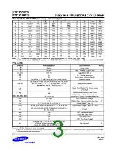
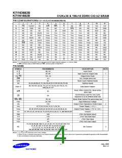
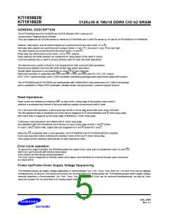
K7I163682B
K7I161882B
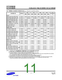
512Kx36 & 1Mx18 DDRII CIO b2 SRAM
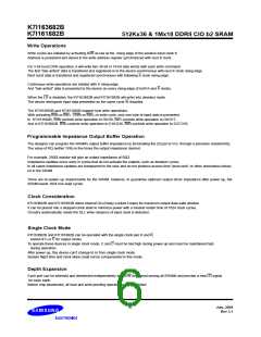
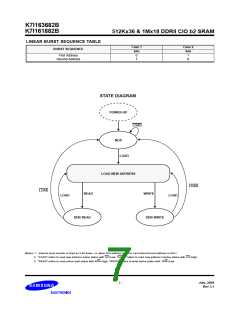
LINEAR BURST SEQUENCE TABLE
Case 1
SA0
Case 2
SA0
BURST SEQUENCE
First Address
Second Address
0
1
1
0
STATE DIAGRAM
POWER-UP
LOAD
NOP
LOAD
LOAD NEW ADDRESS
LOAD
LOAD
READ
LOAD
WRITE
LOAD
DDR READ
DDR WRITE
Notes: 1. Internal burst counter is fixed as 2-bit linear, i.e. when first address is A0+0, next internal burst address is A0+1.
2. "LOAD" refers to read new address active status with LD=Low, "LOAD" refers to read new address inactive status with LD=High.
3. "READ" refers to read active read status with R/W=High, "WRITE" refers to write active status with R/W=Low
July. 2004
Rev 3.1
- 7 -

 SAMSUNG [ SAMSUNG ]