Rev. 1.01
K4B2G0446D
K4B2G0846D
datasheet
DDR3L SDRAM
14.2 Timing Parameter Notes
1. Actual value dependant upon measurement level definitions which are TBD.
2. Commands requiring a locked DLL are: READ (and RAP) and synchronous ODT commands.
3. The max values are system dependent.
4. WR as programmed in mode register
5. Value must be rounded-up to next higher integer value
6. There is no maximum cycle time limit besides the need to satisfy the refresh interval, tREFI.
7. For definition of RTT turn-on time tAON see "Device Operation & Timing Diagram Datasheet"
8. For definition of RTT turn-off time tAOF see "Device Operation & Timing Diagram Datasheet".
9. tWR is defined in ns, for calculation of tWRPDEN it is necessary to round up tWR / tCK to the next integer.
10. WR in clock cycles as programmed in MR0
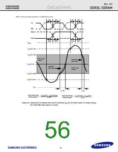
11. The maximum read postamble is bound by tDQSCK(min) plus tQSH(min) on the left side and tHZ(DQS)max on the right side. See "Device Operation & Timing
Diagram Datasheet.
12. Output timing deratings are relative to the SDRAM input clock. When the device is operated with input clock jitter, this parameter needs to be derated
by TBD
13. Value is only valid for RON34
14. Single ended signal parameter. Refer to chapter 8 and chapter 9 for definition and measurement method.
15. tREFI depends on T
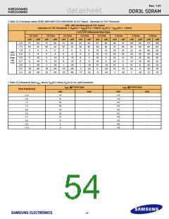
OPER
16. tIS(base) and tIH(base) values are for 1V/ns CMD/ADD single-ended slew rate and 2V/ns CK, CK differential slew rate, Note for DQ and DM signals,
V
(DC) = V DQ(DC). For input only pins except RESET, V (DC)=V CA(DC).
REF
REF
REF
REF
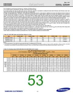
See Address/Command Setup, Hold and Derating : on page 53. .
17. tDS(base) and tDH(base) values are for 1V/ns DQ single-ended slew rate and 2V/ns DQS, DQS differential slew rate. Note for DQ and DM signals,
(DC)= V DQ(DC). For input only pins except RESET, V (DC)=V CA(DC).
V
REF
REF
REF
REF
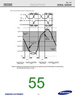
See Data Setup, Hold and Slew Rate Derating : on page 59.
18. Start of internal write transaction is defined as follows ;
For BL8 (fixed by MRS and on-the-fly) : Rising clock edge 4 clock cycles after WL.
For BC4 (on-the-fly) : Rising clock edge 4 clock cycles after WL
For BC4 (fixed by MRS) : Rising clock edge 2 clock cycles after WL
19. The maximum read preamble is bound by tLZDQS(min) on the left side and tDQSCK(max) on the right side. See "Device Operation & Timing Diagram
Datasheet"
20. CKE is allowed to be registered low while operations such as row activation, precharge, autoprecharge or refresh are in progress, but power-down
IDD spec will not be applied until finishing those operations.
21. Although CKE is allowed to be registered LOW after a REFRESH command once tREFPDEN(min) is satisfied, there are cases where additional time
such as tXPDLL(min) is also required. See "Device Operation & Timing Diagram Datasheet".
22. Defined between end of MPR read burst and MRS which reloads MPR or disables MPR function.
23. One ZQCS command can effectively correct a minimum of 0.5 % (ZQCorrection) of RON and RTT impedance error within 64 nCK for all speed bins assuming
the maximum sensitivities specified in the ’Output Driver Voltage and Temperature Sensitivity’ and ’ODT Voltage and Temperature Sensitivity’ tables. The
appropriate interval between ZQCS commands can be determined from these tables and other application specific parameters.
One method for calculating the interval between ZQCS commands, given the temperature (Tdriftrate) and voltage (Vdriftrate) drift rates that the SDRAM is sub-
ject to in the application, is illustrated. The interval could be defined by the following formula:
ZQCorrection
(TSens x Tdriftrate) + (VSens x Vdriftrate)
where TSens = max(dRTTdT, dRONdTM) and VSens = max(dRTTdV, dRONdVM) define the SDRAM temperature and voltage sensitivities.
For example, if TSens = 1.5% /°C, VSens = 0.15% / mV, Tdriftrate = 1°C / sec and Vdriftrate = 15 mV / sec, then the interval between ZQCS commands is calcu-
lated as:
0.5
~
~
128ms
= 0.133
(1.5 x 1) + (0.15 x 15)
24. n = from 13 cycles to 50 cycles. This row defines 38 parameters.
25. tCH(abs) is the absolute instantaneous clock high pulse width, as measured from one rising edge to the following falling edge.
26. tCL(abs) is the absolute instantaneous clock low pulse width, as measured from one falling edge to the following rising edge.
27. The tIS(base) AC150 specifications are adjusted from the tIS(base) specification by adding an additional 100 ps of derating to accommodate for the lower alter-
nate threshold of 150 mV and another 25 ps to account for the earlier reference point [(175 mv - 150 mV) / 1 V/ns].
28. Pulse width of a input signal is defined as the width between the first crossing of V
(DC) and the consecutive crossing of V
(DC)
REF
REF
29. tDQSL describes the instantaneous differential input low pulse width on DQS-DQS, as measured from one falling edge to the next consecutive rising edge.
30. tDQSH describes the instantaneous differential input high pulse width on DQS-DQS, as measured from one rising edge to the next consecutive falling edge.
31. tDQSH, act + tDQSL, act = 1 tCK, act ; with tXYZ, act being the actual measured value of the respective timing parameter in the application.
32. tDSH, act + tDSS, act = 1 tCK, act ; with tXYZ, act being the actual measured value of the respective timing parameter in the application.
- 52 -

 SAMSUNG [ SAMSUNG ]