Rev. 1.01
K4B2G0446D
K4B2G0846D
datasheet
DDR3L SDRAM
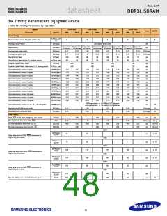
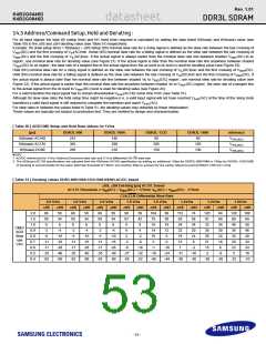
[ Table 49 ] Timing Parameters by Speed Bin (Cont.)
Speed
DDR3-800
DDR3-1066
DDR3-1333
DDR3-1600
Units
NOTE
Parameter
Symbol
MIN
MAX
MIN
MAX
MIN
MAX
MIN
MAX
Reset Timing
max(5nCK,
tRFC +
max(5nCK,
tRFC +
max(5nCK,
tRFC +
max(5nCK,
tRFC +
Exit Reset from CKE HIGH to a valid command
tXPR
-
-
-
-
10ns)
10ns)
10ns)
10ns)
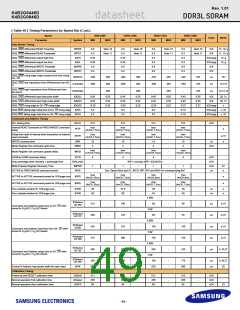
Self Refresh Timing
max(5nCK,t
RFC +
max(5nCK,t
RFC +
max(5nCK,t
RFC +
Exit Self Refresh to commands not requiring a locked
DLL
max(5nCK,t
RFC + 10ns)
tXS
-
-
-
-
10ns)
10ns)
10ns)
Exit Self Refresh to commands requiring a locked DLL
tXSDLL
tCKESR
tDLLK(min)
-
-
tDLLK(min)
-
-
tDLLK(min)
-
-
tDLLK(min)
-
-
nCK
Minimum CKE low width for Self refresh entry to exit
timing
tCKE(min)+
1tCK
tCKE(min)+
1tCK
tCKE(min)+
1tCK
tCKE(min) +
1tCK
Valid Clock Requirement after Self Refresh Entry
(SRE) or Power-Down Entry (PDE)
max(5nCK,
10ns)
max(5nCK,
10ns)
max(5nCK,
10ns)
max(5nCK,
10ns)
tCKSRE
tCKSRX
-
-
-
-
-
-
-
-
Valid Clock Requirement before Self Refresh Exit
(SRX) or Power-Down Exit (PDX) or Reset Exit
max(5nCK,
10ns)
max(5nCK,
10ns)
max(5nCK,
10ns)
max(5nCK,
10ns)
Power Down Timing
Exit Power Down with DLL on to any valid com-
mand;Exit Precharge Power Down with DLL
frozen to commands not requiring a locked DLL
max
max
max
max
tXP
tXPDLL
tCKE
(3nCK,
7.5ns)
-
-
-
(3nCK,
7.5ns)
-
-
-
-
-
-
-
-
-
(3nCK,6ns)
(3nCK,6ns)
max
(10nCK,
24ns)
max
(10nCK,
24ns)
max
(10nCK,
24ns)
max
(10nCK,
24ns)
Exit Precharge Power Down with DLL frozen to com-
mands requiring a locked DLL
2
max
max
max
max
CKE minimum pulse width
(3nCK,
7.5ns)
(3nCK,
5.625ns)
(3nCK,
5.625ns)
(3nCK,5ns)
Command pass disable delay
tCPDED
tPD
1
-
1
-
1
-
1
-
nCK
tCK
Power Down Entry to Exit Timing
tCKE(min)
9*tREFI
tCKE(min)
9*tREFI
tCKE(min)
9*tREFI
tCKE(min)
9*tREFI
15
20
20
Timing of ACT command to Power Down entry
Timing of PRE command to Power Down entry
Timing of RD/RDA command to Power Down entry
tACTPDEN
tPRPDEN
tRDPDEN
1
1
-
-
-
1
1
-
-
-
1
1
-
-
-
1
1
-
-
-
nCK
nCK
RL + 4 +1
RL + 4 +1
RL + 4 +1
RL + 4 +1
WL + 4
+(tWR/
WL + 4
+(tWR/
WL + 4
+(tWR/
WL + 4
+(tWR/
Timing of WR command to Power Down entry
(BL8OTF, BL8MRS, BC4OTF)
tWRPDEN
tWRAPDEN
tWRPDEN
-
-
-
-
-
-
-
-
-
-
-
-
-
-
-
-
nCK
nCK
nCK
nCK
9
10
9
tCK(avg))
tCK(avg))
tCK(avg))
tCK(avg))
Timing of WRA command to Power Down entry
(BL8OTF, BL8MRS, BC4OTF)
WL + 4
WL + 4
WL + 4
WL + 4 +WR
+1
+WR +1
+WR +1
+WR +1
WL + 2
+(tWR/
WL + 2
+(tWR/
WL + 2
+(tWR/
WL + 2
+(tWR/
Timing of WR command to Power Down entry
(BC4MRS)
tCK(avg))
tCK(avg))
tCK(avg))
tCK(avg))
Timing of WRA command to Power Down entry
(BC4MRS)
WL +2 +WR
+1
WL +2 +WR
+1
WL +2 +WR
+1
WL +2 +WR
+1
tWRAPDEN
tREFPDEN
10
Timing of REF command to Power Down entry
Timing of MRS command to Power Down entry
ODT Timing
1
-
-
1
-
-
1
-
-
1
-
-
20,21
tMRSPDEN tMOD(min)
tMOD(min)
tMOD(min)
tMOD(min)
ODT high time without write command or with write
command and BC4
ODTH4
ODTH8
tAONPD
4
6
2
-
-
4
6
2
-
-
4
6
2
-
-
4
6
2
-
-
nCK
nCK
ns
ODT high time with Write command and BL8
Asynchronous RTT turn-on delay (Power-Down with
DLL frozen)
8.5
8.5
8.5
8.5
Asynchronous RTT turn-off delay (Power-Down with
DLL frozen)
tAOFPD
tAON
2
8.5
400
0.7
0.7
2
8.5
300
0.7
0.7
2
8.5
250
0.7
0.7
2
8.5
225
0.7
0.7
ns
RTT turn-on
-400
0.3
0.3
-300
0.3
0.3
-250
0.3
0.3
-225
0.3
0.3
ps
7,f
8,f
f
RTT_NOM and RTT_WR turn-off time from ODTLoff
reference
tAOF
tCK(avg)
tCK(avg)
RTT dynamic change skew
tADC
Write Leveling Timing
First DQS pulse rising edge after tDQSS margining
mode is programmed
tWLMRD
tWLDQSEN
tWLH
40
25
-
-
-
-
40
25
-
-
-
-
40
25
-
-
-
-
40
25
-
-
-
-
tCK
tCK
ps
3
3
DQS/DQS delay after tDQS margining mode is pro-
grammed
Write leveling setup time from rising CK, CK crossing
to rising DQS, DQS crossing
325
325
245
245
195
195
165
165
Write leveling hold time from rising DQS, DQS cross-
ing to rising CK, CK crossing
tWLH
ps
Write leveling output delay
Write leveling output error
tWLO
0
0
9
2
0
0
9
2
0
0
9
2
0
0
7.5
2
ns
ns
tWLOE
- 50 -

 SAMSUNG [ SAMSUNG ]