RT8876A
If then the output voltage is :
Dynamic VID Enhancement
V
= V
−I
×R
+ V
OUT
DAC
LOAD
DROOP PIN−OFS
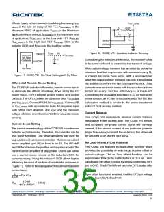
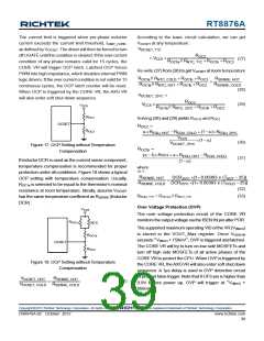
During a dynamic VID event, the charging (dynamic VID
up) or discharging (dynamic VID down) current causes
unwanted load-line effect which degrades the settling time
performance. The DVID pin can be used to compensate
the load-line effect, so that the output voltage can be settled
to the target value more quickly. During a dynamic VIDup
(17)
+ V
SVID−OFS
The pin offset voltage is set by supplying a voltage into
OFS pin. The linear range of offset pin voltage is from
0.9V to 1.83V. The pin offset voltage can be calculated as
below :
event occurred, the RT8876Asources out a current (IDVID
)
VPIN−OFS = VOFS −1.2V
(18)
to DVID pin. The voltage on DVID pin is added to DAC
during DVID rising to enhance the dynamic VID
performance. Connecting a capacitor in parallel with a
resistor toDVIDpin is recommended. IDVID is 8μAduring a
SetVID_Fast event. If it is a SetVID_Slow event, IDVID
automatically shrinks to 2μA (if slow slew rate is 0.25 x
fast slew rate). This function is null during a dynamic VID
down event.
For example, supplying 1.3V at OFS pin will achieve
100mV offset at the output. Connecting a filter capacitor
between the OFS pin and GND is necessary.
Operation Mode Transition
RT8876A supports operation mode transition function at
the CORE VR for the SetPS command of Intel's VR12/
IMVP7 CPU. The default operation mode of the CORE
VR is PS0, which is full phase CCM operation. Other
operation modes include PS1 (single phase CCM
operation) and PS2 (single phase DEM operation). After
receiving SetPS command, the CORE VR will immediately
change to the new operation state. When the CORE VR
receives SetPS command of PS1 operation mode, the
CORE VR operates as a single phase CCM controller,
and only channel 1 is active. The CORE VR will disable
phase 2 and phase 3 by disabling Internal PWM logic
drivers (PWM = high impedance state). Therefore, 2
internal drivers which support tri-state shutdown are also
required for compatibility with PS1 operation mode.
Similarly, when the CORE VR receives SetPS command
of PS2 operation mode, the CORE VR operates as a single
phase DCM controller, and only channel 1 is active with
diode emulation operation. The CORE VR will disable
phase 2 and phase 3 by disabling internal PWM logic
drivers (PWM = high impedance state). Therefore, all
internal drivers which support tri-state shutdown are
required for compatibility with PS2 operation state. If the
CORE VR receives dynamic VID change command
(SetVID), the CORE VR will automatically enter PS0
operation mode and all phases will be activated. After
VOUT,CORE reaches target voltage, the CORE VR will stay
at PS0 state and ignore former SetPS command. Only
re-sending SetPS command after SetVID command will
the CORE VR be forced into PS1 or PS2 operation states
again.
DAC
I
DVID
Slew Rate
Control
DVID
Event
DVID
FB
1/20
+
EA
-
Figure 13.DVIDCompensation Circuit
Ramp Amplitude Adjust
When the CORE VR enters PS2 operation mode, the
internal ramp of CORE VR will be modified for the reason
of stability. In case of smooth transition into PS2, the
CCM ramp amplitude should be designed properly. The
RT8876A provides RSET pin for platform users to set the
ramp amplitude of the CORE VR in CCM. The criteria is
to set the ramp amplitude proportional to the on-time (when
VDAC <1.2V). The equation will be :
57.6 x 10−12 = tON x (VIN − VDAC) x 1 / RSET
(19)
where 57.6 x 10⁻¹² is an internal coefficient of analog
circuit.
According to equation (12), the RSET equation can be
simplified to :
RRSET = 0.4236 x RTON
(20)
Copyright 2012 Richtek Technology Corporation. All rights reserved.
©
is a registered trademark of Richtek Technology Corporation.
www.richtek.com
36
DS8876A-02 October 2012

 RICHTEK [ RICHTEK TECHNOLOGY CORPORATION ]