RT8876A
V
Where fS(MAX) is the maximum switching frequency, tHS-
OUT, CORE
is the turn-on delay of HS-FET, VDAC(MAX) is the
DELAY
L
DCR
Maximum VDAC of application, VIN(MAX) is the Maximum
application Input voltage, ILOAD(MAX) is the maximum load
C
X
R
X
of application, RON_LS-FET is the Low side FET RDS(ON)
,
+ V
-
X
ISENxP
ISENxN
RON_HS-FET is the High side FET RDS(ON) ,DCR is the
inductor DCR, and RDROOP is the load line setting.
R
R1
TON
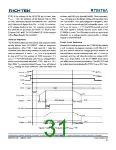
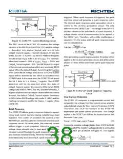
Figure 12. CORE VR : Lossless Inductor Sensing
TONSET
V
IN, CORE
CCRCOT
On-Time
Computer
C1
Considering the inductance tolerance, the resistor RX has
to be tuned on board by examining the transient voltage.
VDAC
On-Time
If the output voltage transient has an initial dip below the
minimum load line requirement with a slow recovery, RX
is chosen too small. Vice versa, with a resistance too
large the output voltage transient has only a small initial
dip and the recovery is too fast causing a ring back. Using
current sense resistor in series with the inductor can have
better accuracy, but the efficiency is a trade-off.
Considering the equivalent inductance (LESL) of the current
sense resistor, an RC filter is recommended. The RC filter
calculation method is similar to the above mentioned
inductorDCR sensing method.
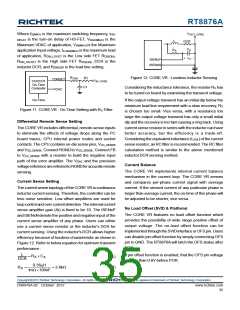
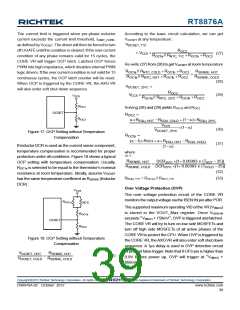
Figure 11. CORE VR : On-Time Setting with RC Filter
Differential Remote Sense Setting
The CORE VR includes differential, remote-sense inputs
to eliminate the effects of voltage drops along the PC
board traces, CPU internal power routes and socket
contacts. The CPU contains on-die sense pins, VCC_SENSE
and VSS_SENSE. Connect RGNDto VSS_SENSE. Connect FB
to VCC_SENSE with a resistor to build the negative input
path of the error amplifier. The VDAC and the precision
voltage reference are referred to RGNDfor accurate remote
sensing.
Current Balance
The CORE VR implements internal current balance
mechanism in the current loop. The CORE VR senses
and compares per-phase current signal with average
current. If the sensed current of any particular phase is
larger than average current, the on-time of this phase will
be adjusted to be shorter, vice versa.
Current Sense Setting
The current sense topology of the CORE VR is continuous
inductor current sensing. Therefore, the controller can be
less noise sensitive. Low offset amplifiers are used for
loop control and over current detection. The internal current
sense amplifier gain (Ai) is fixed to be 10. The ISENxP
and ISENxNdenote the positive and negative input of the
current sense amplifier of any phase. Users can either
use a current sense resistor or the inductor's DCR for
current sensing. Using the inductor's DCR allows higher
efficiency because of lossless characteristic as shown in
Figure 12. Refer to below equation for optimum transient
performance :
No Load Offset (SVID & Platform)
The CORE VR features no load offset function which
provides the possibility of wide range positive offset of
output voltage. The no-load offset function can be
implemented through the SVIDinterface or OFS pin. Users
can disable pin offset function by simply connecting OFS
pin to GND. The RT8876A will latch the OFS status after
POR.
L
DCR
If pin offset function is enabled, that the OFS pin voltage
is more than 0.6V before POR.
= R × C
(15)
(16)
X
X
0.36μH
1m Ω×10 0nF
R
=
= 3.6kΩ
X
Copyright 2012 Richtek Technology Corporation. All rights reserved.
©
is a registered trademark of Richtek Technology Corporation.
DS8876A-02 October 2012
www.richtek.com
35

 RICHTEK [ RICHTEK TECHNOLOGY CORPORATION ]