RT8876A
Since theDCR of the inductor is temperature dependent,
it affects the output accuracy at hot conditions.
Temperature compensation is recommended for the
lossless inductor DCR current sense method. Figure 10
shows a simple but effective way of compensating the
temperature variations of the sense resistor using anNTC
thermistor placed in the feedback path.
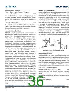
V
IN, CORE
UGATEx
LGATEx
V
OUT, CORE
HS_FET
CCRCOT
PWM
Logic
L
Driver
R
X
C
X
CMP
R
C
LS_FET
C
ISENxP
ISENxN
+
A
I
V
CS
-
C2
C1
C1
Offset
Canceling
C2
R2
R1
R2
COMP
R1b
R1a
COMP
FB
V
CC_SENSE
V
CC_SENSE
FB
-
R
NTC
-
EA
RGND
EA
RGND
V
+
SS_SENSE
V
+
SS_SENSE
V
DAC, CORE
VDAC
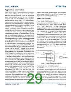
Figure 8. CORE VR : Simplified Schematic for Droop
and Remote Sense in CCM
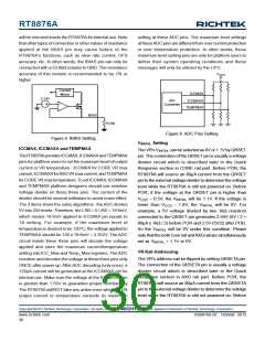
Figure 10. Loop Setting with Temperature
Compensation
Usually, R1a is set to equal RNTC (25°C). R1b is selected
to linearize the NTC's temperature characteristic. For a
given NTC, design is to get R1b and R2 and then C1 and
C2. According to equation (2), to compensate the
temperature variations of the sense resistor, the error
amplifier gain (AV) should have the same temperature
coefficient with RSENSE. Hence
Droop Setting (with Temperature Compensation)
It's very easy to achieveActive Voltage Positioning (AVP)
by properly setting the error amplifier gain due to the native
droop characteristics. The target is to have
VOUT = VDAC − ILOAD x RDROOP
(1)
Then solving the switching condition VCOMP2 = VCS in
Figure 8 yields the desired error amplifier gain AV as
A
R
SENSE, HOT
V, HOT
(3)
=
A
R
SENSE, COLD
V, COLD
A ×R
R2
R1
I
SENSE
A
=
=
(2)
V
From equation (2),AV can be obtained at any temperature
R
DROOP
(T°C) as shown below :
where AI is the internal current sense amplifier gain 10V/
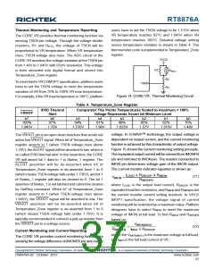
V. RSENSE is the current sense resistor. Figure 9 shows
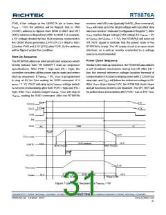
the error amplifier gain (AV) influence on VOUT accuracy
according to equation (2). In general, the DCR of the
inductor is adopted as RSENSE to achieve lossless current
sensing method. RDROOP is the equivalent load line
resistance as well as the desired static output impedance.
R2
A
=
(4)
V, T°C
R1a // R
+ R1b
NTC, T°C
The standard formula for the resistance ofNTC thermistor
as a function of temperature is given by :
⎡
1
1
298
⎤
β
−
(
(
{
⎢
⎣
⎥
⎦
T+273
RNTC, T°C = R25°C
e
(5)
V
OUT
where R25°C is the thermistor's nominal resistance at room
temperature, β is the thermistor's material constant in
Kelvins, and T is the thermistor's actual temperature in
Celsius.
A
> A
V1
V2
A
A
V2
TheDCR value at different temperature can be calculated
by the following equation :
V1
DCRT°C = DCR25°C x [1 + 0.00393 x (T − 25)]
(6)
0
Load Current
where 0.00393 is the temperature coefficient of copper.
For a given NTC thermistor, solving equation (4) at room
temperature (25°C) yields :
Figure 9. ErrorAmplifier gain (AV) Influence on Load Line
Copyright 2012 Richtek Technology Corporation. All rights reserved.
©
is a registered trademark of Richtek Technology Corporation.
DS8876A-02 October 2012
www.richtek.com
33

 RICHTEK [ RICHTEK TECHNOLOGY CORPORATION ]