RT8876A
R2 = AV, 25°C x (R1b + R1a // RNTC, 25°C
)
(7)
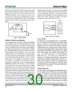
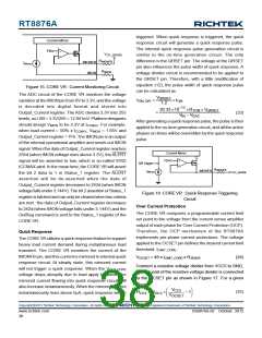
on time control is adopted in RT8876A, a constant on
time can be set by connecting a resistor from VIN to
TONSET pin first, and then the switching frequency of the
regulator can be decided to apply in different applications.
Figure 11 shows the On-Time setting Circuit. Connect a
resistor (RTON) between VIN,CORE and TONSET to set the
whereAV, 25°C is the error amplifier gain at room temperature
and can be obtained from equation (2). R1b can be obtained
by substituting (7) for (3),
R1b =
RSENSE, HOT
×(R1a / /RNTC, HOT ) − (R1a // RNTC, COLD
RSENSE, COLD
)
on-time of UGATE :
−12
24.4×10
×R
TON
RSENSE, HOT
⎛
⎜
⎝
⎞
⎟
⎠
(12)
t
(V
DAC
< 1.2V) =
ON
1−
V
IN
− V
RSENSE, COLD
DAC
(8)
where tON is the UGATE turn on period, VIN is Input voltage
of the CORE VR, and VDAC is the DAC voltage. When
VDAC is larger than 1.2V, the equivalent switching
frequency may be over 500kHz, and this too fast switching
frequency is unacceptable. Therefore, the CORE VR
implements a pseudo constant frequency technology to
avoid this disadvantage of CCRCOT topology. When VDAC
is larger than 1.2V, the on-time equation will be modified
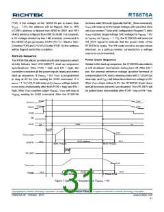
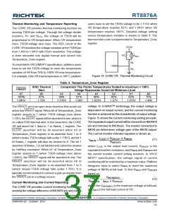
Loop Compensation
Optimized compensation of the CORE VR allows for best
possible load step response of the regulator's output. A
type-I compensator with one pole and one zero is adequate
for proper compensation. Figure 10 shows the
compensation circuit. Previous design procedure shows
how to select resistive feedback components for the error
amplifier gain. Next, C1 and C2 must be calculated for
compensation. The target is to achieve constant resistive
output impedance over the widest possible frequency
range. The pole frequency of the compensator must be
set to compensate the output capacitor ESR zero :
to :
−12
20.33×10
×R
× V
TON DAC
t
(V
DAC
≥ 1.2V) =
ON
V
IN
− V
(13)
DAC
During PS2/PS3 operation, the CORE VR shrinks its on-
time for the purpose of reducing output voltage ripple
caused byDCM operation. The shrink percentage is 15%
compared with original on-time setting by equation (12)
or (13). That is, after setting the PS0 operation on-time,
the PS2/PS3 operation on-time is 0.85 times the original
on-time. On-time translates only roughly to switching
frequencies. The on-times guaranteed in the Electrical
Characteristics are influenced by switching delays in
external HS-FET. Also, the dead-time effect increases the
effective on-time, which in turn reduces the switching
frequency. It occurs only in CCM and during dynamic output
voltage transitions, when the inductor current reverses at
light or negative load currents. With reversed inductor
current, the phase goes high earlier than normal, extending
the on-time by a period equal to the HS-FET rising dead
time. For better efficiency of the given load range, the
maximum switching frequency is suggested to be :
1
1
(9)
fP =
2× π× C×RC
where C is the capacitance of output capacitor, and RC is
the ESR of output capacitor. C2 can be calculated as
follows :
C×R
R2
C
(10)
C2 =
The zero of compensator has to be placed at half of the
switching frequency to filter the switching related noise.
Such that,
1
C1 =
(11)
R1b + R1a // R
× π× f
SW
(
)
NTC, 25°C
TON Setting
High frequency operation optimizes the application for the
smaller component size, trading off efficiency due to higher
switching related losses. This may be acceptable in ultra
portable devices where the load currents are lower and
the controller is powered from a lower voltage supply. Low
frequency operation offers the best overall efficiency at
the expense of component size and board space. Constant
fS(MAX)(kHz) =
×
TON − THS−Delay
⎡
⎤
VDAC(MAX) +ILOAD(MAX) × RON_LS−FET + DCR − RDROOP
⎣
⎦
⎡ ⎤
+ILOAD(MAX) × RON_LS−FET −RON_HS−FET
V
IN(MAX)
⎣
⎦
(14)
Copyright 2012 Richtek Technology Corporation. All rights reserved.
©
is a registered trademark of Richtek Technology Corporation.
www.richtek.com
34
DS8876A-02 October 2012

 RICHTEK [ RICHTEK TECHNOLOGY CORPORATION ]