RT8876A
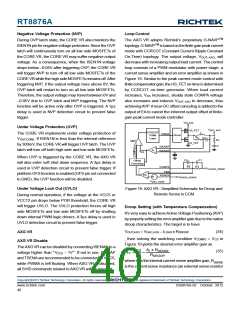
Negative Voltage Protection (NVP)
Loop Control
During OVP latch state, the CORE VR also monitors the
ISEN1N pin for negative voltage protection. Since the OVP
latch will continuously turn on all low side MOSFETs of
the CORE VR, the CORE VR may suffer negative output
voltage. As a consequence, when the ISEN1N voltage
drops below −0.05V after triggering OVP, the CORE VR
will trigger NVP to turn off all low side MOSFETs of the
CORE VR while the high side MOSFETs remains off.After
triggering NVP, if the output voltage rises above 0V, the
OVP latch will restart to turn on all low side MOSFETs.
Therefore, the output voltage may travel between 0V and
−0.05V due to OVP latch and NVP triggering. The NVP
function will be active only after OVP is triggered. A 1μs
delay is used in NVP detection circuit to prevent false
trigger.
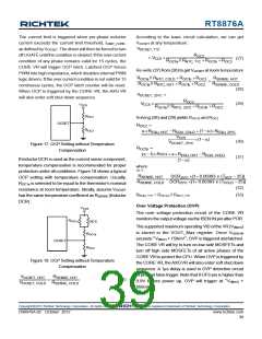
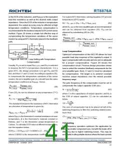
The AXG VR adopts Richtek's proprietary G-NAVPTM
topology.G-NAVPTM is based on the finite gain peak current
mode with CCRCOT (Constant Current Ripple Constant
On-Time) topology. The output voltage, VOUT, AXG, will
decrease with increasing output load current. The control
loop consists of a PWM modulator with power stage, a
current sense amplifier and an error amplifier as shown in
Figure 19. Similar to the peak current mode control with
finite compensator gain, the HS_FET on-time is determined
by CCRCOT on-time generator. When load current
increases, VCS increases, steady state COMPA voltage
also increases and induces VOUT, AXG to decrease, thus
achievingAVP.Anear-DC offset canceling is added to the
output of EA to cancel the inherent output offset of finite-
gain peak current mode controller.
V
IN, AXG
Under Voltage Protection (UVP)
V
OUT, AXG
HS_FET
CCRCOT
PWM
Logic
L
The CORE VR implements under voltage protection of
PWMA
Driver
R
X
C
X
VOUT,CORE. If ISEN1N is less than the internal reference
R
C
CMP
LS_FET
by 300mV, the CORE VR will trigger UVP latch. The UVP
latch will turn off both high side and low side MOSFETs.
C
ISENAP
ISENAN
+
A
I
V
CS
-
When UVP is triggered by the CORE VR, the AXG VR
will also enter soft shut down sequence. A 3μs delay is
used in UVP detection circuit to prevent false trigger. If
platform OFS function is enabled (OFS pin not connected
to GND), the UVP function will be disabled.
C1
R1
C2
Offset
Canceling
R2
COMPA
V
CCAXG_SENSE
FBA
-
EA
RGNDA
V
+
SSAXG_SENSE
V
DAC, CORE
Under Voltage Lock Out (UVLO)
Figure 19. AXGVR : Simplified Schematic for Droop and
Remote Sense in CCM
During normal operation, if the voltage at the VCC5 or
VCC12 pin drops below POR threshold, the CORE VR
will trigger UVLO. The UVLO protection forces all high
side MOSFETs and low side MOSFETs off by shutting
down internal PWM logic drivers. A 3μs delay is used in
UVLO detection circuit to prevent false trigger.
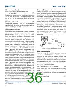
Droop Setting (with Temperature Compensation)
It's very easy to achieveActive Voltage Positioning (AVP)
by properly setting the error amplifier gain due to the native
droop characteristics. The target is to have
VOUT,AXG = VDAC,AXG − ILOAD x RDROOP
(34)
AXG VR
, then solving the switching condition VCOMP2 = VCS in
Figure 19 yields the desired error amplifier gain as
AXG VR Disable
TheAXGVR can be disabled by connecting ISENANto a
voltage higher than “VCC5 − 1V”. If not in use, ISENAP
and TSENAare recommended to be connected to VCC5,
while PWMA is left floating. When AXG VR is disabled,
all SVID commands related to AXG VR will be rejected.
A x R
R2
R1
I
SENSE
(35)
A
=
=
V
R
DROOP
whereAI is the internal current sense amplifier gain, RSENSE
is the current sense resistance (an external sense resistor
Copyright 2012 Richtek Technology Corporation. All rights reserved.
©
is a registered trademark of Richtek Technology Corporation.
www.richtek.com
40
DS8876A-02 October 2012

 RICHTEK [ RICHTEK TECHNOLOGY CORPORATION ]