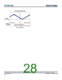
RT8876A
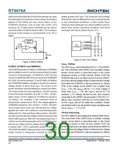
4V
3.5V
3.7V
VCC12
VCC5
4.2V
POR
EN
SVID
Valid
xx
XX
2ms
V
= 1.1V
INITIAL
0.2V
V
OUT,CORE
Hi-Z
SVID defined
Hi-Z
UGATE
MAX Phases
100µs
MAX Phases
VR_RDY
V
= 1.1V
INITIAL
0.2V
V
OUT,AXG
Hi-Z
SVID defined
Hi-Z
PWMA
1 Phase CCM
1 Phase CCM
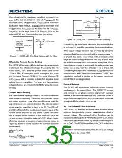
Figure 7 (b). Power Sequence for VINITIAL = 1.1V
CORE VR
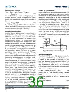
Loop Control Introduction
The CORE VR adopts Richtek's proprietary G-NAVPTM
topology.G-NAVPTM is based on the finite gain peak current
mode with CCRCOT (Constant Current Ripple Constant
On-Time) topology. The control loop consists of PWM
modulators with power stages, current sense amplifiers
and an error amplifier as shown in Figure 8. Similar to the
peak current mode control with finite compensator gain,
the HS_FET on-time is determined by CCRCOT on-time
generator. When load current increases, VCS increases,
the steady state COMP voltage also increases and induces
VOUT,CORE to decrease, thus achievingAVP to meet Intel's
load line specification.Anear-DC offset canceling is added
to the output of EA to eliminate the inherent output offset
of finite gain peak current mode controller.
Active Phase Determination : Before POR
The number of active phases is determined by the internal
circuitry that monitors the ISENxN voltages during start-
up. Normally, the CORE VR operates as a 3-phase PWM
controller. Pulling ISEN3N to VCC5 programs a 2-phase
operation, pulling ISEN3Nand ISEN2Nto VCC5 programs
a 1-phase operation. Before POR, CORE VR detects
whether the voltages of ISEN2N and ISEN3N are higher
than “VCC5 − 1V” respectively to decide how many
phases should be active. Phase selection is only active
during POR. When POR = high, the number of active
phases is determined and latched. The unused ISENxP
pins are recommended to be connected to VCC5.
Copyright 2012 Richtek Technology Corporation. All rights reserved.
©
is a registered trademark of Richtek Technology Corporation.
www.richtek.com
32
DS8876A-02 October 2012

 RICHTEK [ RICHTEK TECHNOLOGY CORPORATION ]