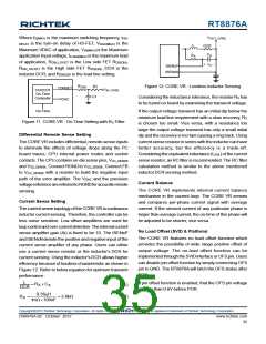
RT8876A
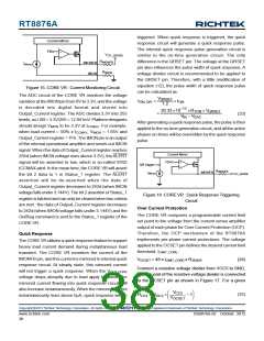
The current limit is triggered when per-phase inductor
current exceeds the current limit threshold, ILIMIT_CORE
According to the basic circuit calculation, we can get
VOCSET at any temperature :
,
VOCSET, T°C
as defined by VOCSET. The driver will then be forced to turn
off UGATE until the condition is cleared. If the over current
condition of any phase remains valid for 15 cycles, the
CORE VR will trigger OCP latch. Latched OCP forces
PWM into high impedance, which disables internal PWM
logic drivers. If the over current condition is not valid for 15
continuous cycles, the OCP latch counter will be reset.
When OCP is triggered by the CORE VR, the AXG VR
will also enter soft shut down sequence.
ROC2
= VCC5
×
(27)
ROC1a // RNTC, T°C + ROC1b + ROC2
Re-write (27) from (26) to get VOCSET at room temperature
R
// R
+ R
+ R
+ R
+ R
R
SENSE, HOT
OC1a
NTC, COLD
OC1b
OC2
=
R
// R
R
SENSE, COLD
OC1a
NTC, HOT
OC1b
OC2
(28)
VOCSET, 25°C
VCC5
=
ROC2
×
(29)
V
CC5
ROC1a // RNTC, 25°C + ROC1b + ROC2
R
OC1
Solving (28) and (29) yields ROC1b and ROC2
ROC2
OCSET
=
R
OC2
α ×REQU, HOT −REQU, COLD + (1− α)×REQU, 25°C
VCC5
VOCSET, 25°C
×(1− α)
(30)
(31)
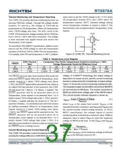
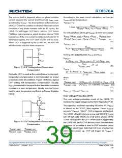
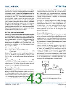
Figure 17. OCP Setting without Temperature
Compensation
ROC1b
=
(α −1)×ROC2 + α ×REQU, HOT − REQU, COLD
(1− α)
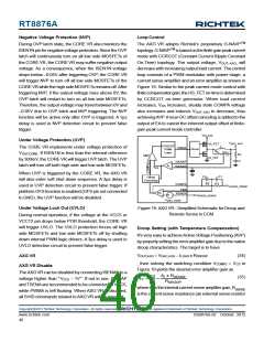
If inductorDCR is used as the current sense component,
temperature compensation is recommended for proper
protection under all conditions. Figure 18 shows a typical
OCP setting with temperature compensation. Usually,
ROC1a is selected to be equal to the thermistor's nominal
resistance at room temperature. Ideally, assume VOCSET
has the same temperature coefficient as RSENSE (Inductor
DCR) :
where
α =
RSENSE, HOT
DCR25°C ×[1+ 0.00393 x (THOT − 25)]
RSENSE, COLD DCR25°C ×[1+ 0.00393 x (TCOLD − 25)]
=
(32)
REQU, T°C = ROC1a // RNTC, T°C
(33)
Over Voltage Protection (OVP)
V
CC5
The over voltage protection circuit of the CORE VR
monitors the output voltage via the ISEN1N pin after POR.
R
OC1a
NTC
OC1b
The supported maximum operating VID of the VR (V(MAX)
)
is stored in the VOUT_Max register. Once VISEN1N
exceeds “V(MAX) + 150mV”, OVP is triggered and latched.
The CORE VR will try to turn on low side MOSFETs and
turn off high side MOSFETs of all active phases of the
CORE VR to protect the CPU. When OVP is triggered by
the CORE VR, theAXGVR will also enter soft shut down
sequence. A 1μs delay is used in OVP detection circuit
to prevent false trigger. Note that if OFS pin is higher than
R
R
OCSET
OC2
Figure 18. OCP Setting without Temperature
Compensation
V
R
SENSE, HOT
OCSET, HOT
=
(26)
0.9V before power up, OVP will trigger at “V(MAX)
850mV”.
+
V
R
SENSE, COLD
OCSET, COLD
Copyright 2012 Richtek Technology Corporation. All rights reserved.
©
is a registered trademark of Richtek Technology Corporation.
DS8876A-02 October 2012
www.richtek.com
39

 RICHTEK [ RICHTEK TECHNOLOGY CORPORATION ]