RT8876A
POR, if the voltage at the QRSETA pin is lower than
− 1.8V, the address will be flipped, that is, VR0
receives valid VIDcode (typically SetVID_Slow command),
VOUT will ramp up to the target voltage with specified slew
rate (see section “Data and Configuration Register”).After
VOUT reaches target voltage (VIDvoltage for VINITIAL = 0V
or VINITIAL for VINITIAL = 1.1V), the RT8876A will send out
VR_RDY signal to indicate that the power state of the
RT8876A is ready. The VR ready circuit is an open-drain
structure, so a pull-up resistor connected to a voltage
source is recommended.
V
CC5
(CORE) address is flipped from 0000 to 0001 and VR1
(AXG) address is flipped from 0001 to 0000. For example,
a 5V voltage divided by two 1kΩ resistors connected to
the QRSETA pin generates 2.54V (5V / 2 + 80μA x 1kΩ /
2) before POR and 2.5V (5V/2) after POR. So the address
will be flipped under this condition.
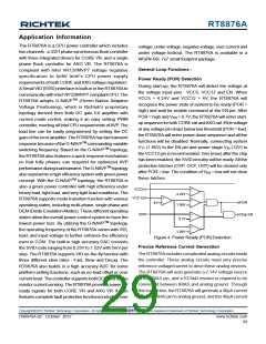
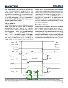
Start-Up Sequence
Power Down Sequence
The RT8876Autilizes an internal soft-start sequence which
strictly follows Intel VR12/IMVP7 start-up sequence
specifications. After POR = high and EN = high, the
controller considers all the power inputs ready and enters
start-up sequence. If VINITIAL = 0V, VOUT is programmed
to stay at 0V for 2ms waiting for SVID command. If V
INITIAL = 1.1V, VOUT will ramp up to VINITIAL voltage (which
is not zero) immediately after both POR = high and EN =
high. After VOUT reaches target VINITIAL, VOUT will stay at
VINITIAL waiting for SVID command. After the RT8876A
Similar to the start-up sequence, the RT8876A also utilizes
a soft shutdown mechanism during turn-off. After EN =
low, the internal reference voltage (positive terminal of
compensation EA) starts ramping down with 3.125mV/μs
slew rate, and VOUT will follow the reference voltage to 0V.
After VOUT drops below 0.2V, the RT8876A shuts down
and all functions (drivers) are disabled. The VR_RDY will
be pulled down immediately after POR = low or EN= low.
4V
3.5V
3.7V
VCC12
4.2V
VCC5
POR
EN
SVID
Valid
xx
XX
2ms
0.2V
V
OUT,CORE
Hi-Z
SVID defined
Hi-Z
UGATE
MAX Phases
100µs
MAX Phases
VR_RDY
0.2V
V
OUT,AXG
Hi-Z
SVID defined
Hi-Z
PWMA
1 Phase CCM
1 Phase CCM
Figure 7 (a). Power Sequence for VINITIAL = 0V
Copyright 2012 Richtek Technology Corporation. All rights reserved.
©
is a registered trademark of Richtek Technology Corporation.
DS8876A-02 October 2012
www.richtek.com
31

 RICHTEK [ RICHTEK TECHNOLOGY CORPORATION ]