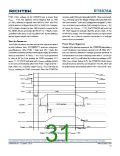
RT8876A
will be mirrored inside the RT8876Afor internal use. Note
that other types of connection or other values of resistance
applied at the IBIAS pin may cause failure of the
RT8876A's functions, such as slew rate control, OFS
accuracy, etc. In other words, the IBIAS pin can only be
connected with a 53.6kΩ resistor toGND. The resistance
accuracy of this resistor is recommended to be 1% or
higher.
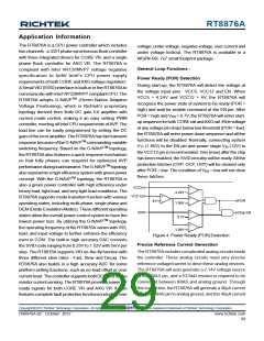
setting at these ADC pins. The maximum level settings
at theseADC pins are different from over current protection
or over temperature protection. In other words, these
maximum level setting pins are only for platform users to
define their system operating conditions and these
messages will only be utilized by the CPU.
V
CC5
Current
Mirror
ICCMAX
2.14V
A/D
Converter
ICCMAXA
TEMPMAX
+
-
IBIAS
53.6k
I
Figure 6. ADC Pins Setting
VINITIAL Setting
Figure 5. IBIAS Setting
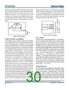
ICCMAX, ICCMAXA and TEMPMAX
The VR's VINITIAL can be selected as 0V or 1.1V by QRSET
pin. The connection of the QRSET pin is usually a voltage
divider circuit which is described later in the Quick
Response section in CORE rail part. Before POR, the
RT8876A will source an 80μA current from the QRSET
pin to the external voltage divider to determine the voltage
level while the RT8876A is still not powered on. Before
POR, if the voltage at the QRSET pin is higher than
The RT8876Aprovides ICCMAX, ICCMAXAandTEMPMAX
pins for platform users to set the maximum level of output
current or VR temperature : ICCMAX for CORE VR max
current, ICCMAXAforAXGVR max current, andTEMPMAX
for CORE VR max temperature. To set ICCMAX, ICCMAXA
and TEMPMAX platform designers should use resistive
voltage divider on these three pins. The current of the
divider should be several milliamps to avoid noise effect.
The 3 items share the same algorithms : theADC divides
5V into 255 levels. Therefore, the LSB = 5 / 255 = 19.6mV,
which means 19.6mV applied to ICCMAX pin equals to
1A setting. For example, if the maximum level of
temperature is desired to be 120°C, the voltage applied to
TEMPMAX should be 120 x 19.6mV = 2.352V. The ADC
circuit inside these three pins will decode the voltage
applied and store the maximum current/temperature
setting into ICC_Max and Temp_Max registers. TheADC
monitors and decodes the voltage at these three pins only
ONCE after power up. AfterADC decoding (only once), a
128μA current will be generated at the ICCMAXA pin for
internal use. Make sure the voltage at the ICCMAXA pin
is greater than 1.55V to guarantee proper functionality
The RT8876AwillNOT take any action even when the VR
output current or temperature exceeds its maximum
V
CC5
− 0.5V, the VINITIAL will be 1.1V. If the voltage is
lower than V
− 1.8V, the VINITIAL will be 0V. For
CC5
example, a 5V voltage divided by two 1kΩ resistors
connected to the QRSET pin generates 2.54V (5V / 2 +
80μA x 1kΩ / 2) before POR and 2.5V (5V/2) after POR.
So the VINITIAL will be 0V under this condition. Please
note that the both Core rail andAXGrail are simultaneously
set as VINITIAL = 1.1V or 0V.
VR Rail Addressing
The VR's address can be flipped by setting QRSETApin.
The connection of the QRSETA pin is usually a voltage
divider circuit which is described later in the Quick
Response section in AXG rail part. Before POR, the
RT8876A will source an 80μA current from the QRSETA
pin to the external voltage divider to determine the voltage
level while the RT8876A is still not powered on. Before
Copyright 2012 Richtek Technology Corporation. All rights reserved.
©
is a registered trademark of Richtek Technology Corporation.
www.richtek.com
30
DS8876A-02 October 2012

 RICHTEK [ RICHTEK TECHNOLOGY CORPORATION ]