R8C/13 Group
13. Serial Interface
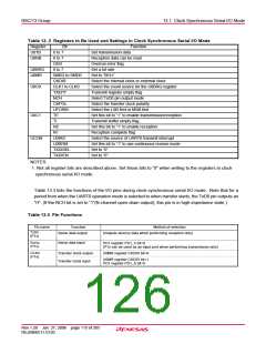
UARTi transmit/receive control register 1 (i=0, 1)
b7 b6 b5 b4 b3 b2 b1 b0
Symbol
U0C1
U1C1
Address
00A516
00AD16
After reset
0216
0216
Bit
symbol
Function
Bit name
RW
TE
TI
Transmit enable bit
0 : Transmission disabled
1 : Transmission enabled
RW
RO
Transmit buffer
empty flag
0 : Data present in UiTB register
1 : No data present in UiTB register
Receive enable bit(1)
Receive complete flag(2)
Nothing is assigned.
RE
RI
0 : Reception disabled
1 : Reception enabled
RW
RO
0 : No data present in UiRB register
1 : Data present in UiRB register
(b7-b4)
When write, set “0”. When read, its content is “0”.
NOTES:
1. As for the UART1, set the TXD1EN bit in the UCON register before setting this bit to reception enabled.
2. The RI bit is set to "0" when the higher byte of the UiRB register is read.
UART transmit/receive control register 2
b7 b6 b5 b4 b3 b2 b1 b0
Symbol
UCON
Address
00B016
After reset
0016
0
0
Bit
symbol
Function
Bit name
RW
RW
U0IRS
U1IRS
UART0 transmit
0 : Transmit buffer empty (Tl = 1)
interrupt cause select bit 1 : Transmission completed (TXEPT = 1)
UART1 transmit
0 : Transmit buffer empty (Tl = 1)
RW
interrupt cause select bit 1 : Transmission completed (TXEPT = 1)
U0RRM UART0 continuous
receive mode enable bit
0 : Continuous receive mode disabled
1 : Continuous receive mode enable
RW
RW
RW
Must set to “0”
Reserved bit
(b4-b3)
Port TxD11 switching bit(2)
0 : I/O port P0
0
TXD1SEL
1 : TxD11
TXD1EN TxD10/RxD
1
0 : RxD
1 : TxD10
1
RW
select bit(1, 2)
Nothing is assigned.
When write, set “0”. When read, its content is “0”.
(b7)
NOTES:
1. For P3
7
, select “0” (RxD1) for data receive, and “1” (TxD10) for data transfer.
Set the PD3_7 bit in the PD3 register to “0” (input mode) when receiving.
2. Do not set the TXD1SEL and TXD1EN bits to “1” at the same time since they function independently.
Figure 13.5 U0C1 and U1C1 Registers and UCON Register
Rev.1.20 Jan 27, 2006 page 113 of 205
REJ09B0111-0120

 RENESAS [ RENESAS TECHNOLOGY CORP ]