R8C/13 Group
13.1 Clock Synchronous Serial I/O Mode
13.1 Clock Synchronous Serial I/O Mode
The clock synchronous serial I/O mode uses a transfer clock to transmit and receive data. This mode can
be selected with UART0. Table 13.1 lists the specifications of the clock synchronous serial I/O mode.
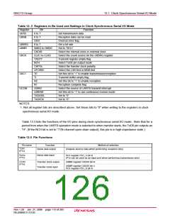
Table 13.2 lists the registers used in clock synchronous serial I/O mode and the register values set.
Table 13.1 Clock Synchronous Serial I/O Mode Specifications
Item
Specification
Transfer data format
Transfer clock
• Transfer data length: 8 bits
• CKDIR bit in U0MR register is set to “0” (internal clock): fi/(2(n+1))
n=setting value in UiBRG register: 0016 to FF16
• CKDIR bit is set to “1” (external clock ): input from CLK0 pin
fi=f1SIO, f8SIO, f32SIO
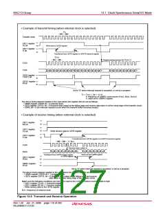
Transmission start condition • Before transmission can start, the following requirements must be met(1)
_ TE bit in U0C1 register is set to “1” (transmission enabled)
_ TI bit in U0C1 register is set to “0” (data present in U0TB register)
Reception start condition
• Before reception can start, the following requirements must be met(1)
_ RE bit in U0C1 register is set to “1” (reception enabled)
_ TE bit in U0C1 register is set to “1” (transmission enabled)
_ TI bit in U0C1 register is set to “0” (data present in the U0TB register)
• For transmission, one of the following conditions can be selected
_ U0IRS bit is set to “0” (transmit buffer empty): when transferring data from
U0TB register to UART0 transmit register (at start of transmission)
_ U0IRS bit is set to “1” (transfer completed): when serial interface finished sending
data from UARTi transmit register
Interrupt request
generation timing
• For reception
When transferring data from the UART0 receive register to the U0RB register (at
completion of reception)
Error detection
Select function
• Overrun error(2)
This error occurs if serial interface started receiving the next data before reading the
U0RB register and received the 7th bit of the next data
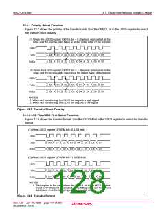
• CLK polarity selection
Transfer data I/O can be chosen to occur synchronously with the rising or
the falling edge of the transfer clock
• LSB first, MSB first selection
Whether to start sending/receiving data beginning with bit 0 or beginning with bit 7
can be selected
• Continuous receive mode selection
Reception is enabled immediately by reading the U0RB register
NOTES:
1. When an external clock is selected, the conditions must be met while if the U0C0 register0 CKPOL bit =
0 (transmit data output at the falling edge and the receive data taken in at the rising edge of the transfer
clock), the external clock is in the high state; if the CKPOL bit in the U0C0 register is set to “1” (transmit
data output at the rising edge and the receive data taken in at the falling edge of the transfer clock), the
external clock is in the low state.
2. If an overrun error occurs, the value of U0RB register will be indeterminate. The IR bit of S0RIC register
does not change.
Rev.1.20 Jan 27, 2006 page 114 of 205
REJ09B0111-0120

 RENESAS [ RENESAS TECHNOLOGY CORP ]