R8C/13 Group
13. Serial Interface
UARTi transmit buffer register(1, 2) (i=0, 1)
Symbol
U0TB
U1TB
Address
00A316-00A216
00AB16-00AA16
After reset
Indeterminate
Indeterminate
(b15)
b7
(b8)
b0 b7
b0
Bit
Function
RW
WO
symbol
(b8-b0)
(b15-b9)
Transmit data
Nothing is assigned.
When write, set to “0”. When read, its content is indeterminate.
NOTES:
1. When transfer data length is 9-bit long, write high-byte first then low-byte.
2. Use MOV instruction to write to this register.
UARTi receive buffer register(1) (i=0, 1)
(b8)
b0 b7
(b15)
b7
Symbol
U0RB
U1RB
Address
00A716-00A616
00AF16-00AE16
After reset
Indeterminate
Indeterminate
b0
Bit
symbol
Function
Bit name
RW
Receive data (D
7
to D
0
)
RO
RO
(b7-b0)
(b8)
Receive data (D
8
)
Nothing is assigned.
When write, set to “0”. When read, its content is indeterminate.
(b11-b9)
OER
Overrun error flag(2)
0 : No overrun error
RO
1 : Overrun error found
Framing error flag(2)
Parity error flag(2)
Error sum flag(2)
FER
PER
SUM
0 : No framing error
1 : Framing error found
RO
RO
0 : No parity error
1 : Parity error found
0 : No error
1 : Error found
RO
NOTES:
1. Read the UiRB register in 16-bit unit.
2. All of the SUM, PER, FER and OER bits are set to “0” (no error) when the SMD2 to SMD0 bits in the UiMR register are set to “000
2” (serial I/O
disabled) or the RE bit in the UiC1 register is set to “0” (reception disabled). The SUM bit is set to “0” (no error) when all of the PER, FER and OER
bits are set to “0” (no error).
The PER and FER bits are set to “0” even when the higher byte of the UiRB register is read.
UARTi bit rate register(1, 2, 3) (i=0, 1)
Symbol
U0BRG
U1BRG
Address
00A116
00A916
After reset
Indeterminate
Indeterminate
b7
b0
Function
Setting range
0016 to FF16
RW
WO
Assuming that set value = n, UiBRG divides the count source
by n + 1
NOTES:
1. Write to this register while serial interface is neither transmitting nor receiving.
2. Use MOV instruction to write to this register.
3. After setting the CLK0 to CLK1 bits of the UiC0 register, write to the UiBRG register.
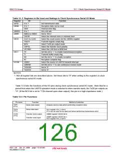
Figure 13.3 U0TB and U1TB Registers, U0RB and U1RB Registers, and U0BRG and U1BRG Registers
Rev.1.20 Jan 27, 2006 page 111 of 205
REJ09B0111-0120

 RENESAS [ RENESAS TECHNOLOGY CORP ]