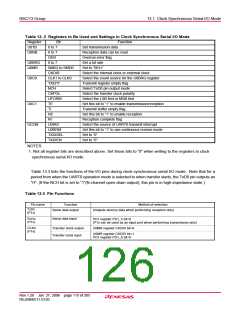
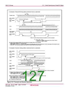
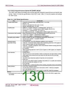
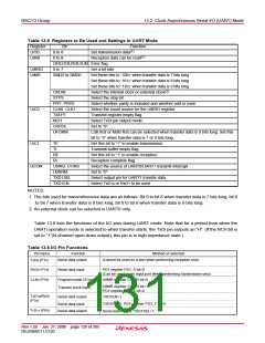
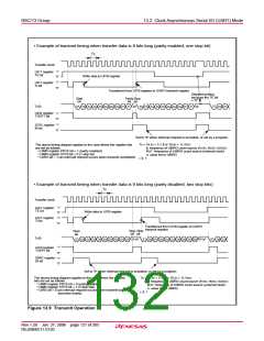
R8C/13 Group
13.1 Clock Synchronous Serial I/O Mode
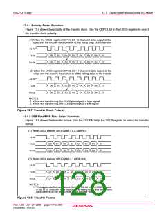
13.1.1 Polarity Select Function
Figure 13.7 shows the polarity of the transfer clock. Use the CKPOL bit in the U0C0 register to select
the transfer clock polarity.
(1) When the U0C0 register CKPOL bit = 0 (transmit data output at the
edge and the receive data taken in at the rising edge of the transfer
CLK0(1)
D0
D
1
D
2
D
3
D
4
D
5
D
6
D7
TXD0
D
0
D
1
D
2
D
3
D
4
D
5
D
6
D7
RXD0
(2) When the U0C0 register CKPOL bit = 1 (transmit data output at the
edge and the receive data taken in at the falling edge of the transfe
CLK0(2)
D
D
0
0
D
1
D
2
D
3
D
4
D
5
D
6
D7
TXD0
D
1
D
2
D
3
D
4
D
5
D
6
D7
RXD0
NOTES:
1. When not transferring, the CLK0 pin outputs a high signal.
2. When not transferring, the CLK0 pin outputs a low signal.
Figure 13.7 Transfer Clock Polarity
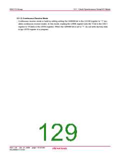
13.1.2 LSB First/MSB First Select Function
Figure 13.8 shows the transfer format. Use the UFORM bit in the U0C0 register to select the transfer
format.
(1) When U0C0 register UFORM bit = 0 (LSB first)
CLK
0
D0
D
1
D
2
D
3
D
4
D
5
D
6
D7
TXD
0
D
1
D
2
D
3
D
4
D
5
D
6
D7
D
0
RXD0
(2) When U0C0 register UFORM bit = 1 (MSB first)
CLK
0
D
D
7
7
D
6
D
5
D
4
D
3
D
2
D
1
D0
TXD
0
D
6
D
5
D
4
D
3
D
2
D
1
D0
RXD0
NOTES:
1. This applies to the case where the CKPOL bit in the U0C0 register
is set to “0” (transmit data output at the falling edge and the receive
data taken in at the rising edge of the transfer clock).
Figure 13.8 Transfer Format
Rev.1.20 Jan 27, 2006 page 117 of 205
REJ09B0111-0120

 RENESAS [ RENESAS TECHNOLOGY CORP ]