R8C/13 Group
13. Serial Interface
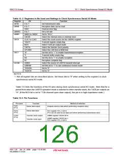
UARTi transmit/receive mode register (i=0, 1)
b7 b6 b5 b4 b3 b2 b1 b0
Symbol
U0MR
U1MR
Address
00A016
00A816
After reset
0016
0016
0
Bit
symbol
Function
Bit name
RW
RW
b2 b1 b0
SMD0
SMD1
Serial interface mode
select bit(2)
0 0 0 : Serial interface disabled
0 0 1 : Clock synchronous serial I/O mode
1 0 0 : UART mode transfer data 7 bits long
1 0 1 : UART mode transfer data 8 bits long
1 1 0 : UART mode transfer data 9 bits long
Must not be set except above
RW
RW
RW
RW
RW
SMD2
Internal/external clock
select bit(3)
0 : Internal clock
1 : External clock(1)
CKDIR
STPS
0 : 1 stop bit
1 : 2 stop bits
Stop bit length select bit
Odd/even parity select bit
PRY
Effective when PRYE = 1
0 : Odd parity
1 : Even parity
0 : Parity disabled
1 : Parity enabled
PRYE
(b7)
Parity enable bit
Reserved bit
RW
RW
Must set to “0”
NOTES:
1. Must set the P1_6 bit in the PD1 register to “0” (input).
2. For the U1MR register, the SMD2 to SMD0 bits must not be set except the followings: “000
2”, “1002”, “1012”, or “1102”.
3. Must set the CKDIR bit to “0” (internal clock) in UART1.
UARTi transmit/receive control register 0 (i=0, 1)
b7 b6 b5 b4 b3 b2 b1 b0
Symbol
U0C0
U1C0
Address
00A416
00AC16
After reset
0816
0
0816
Bit
symbol
Bit name
Function
RW
b1 b0
CLK0
CLK1
BRG count source
select bit(1)
0 0 : f1SIO is selected
0 1 : f8SIO is selected
1 0 : f32SIO is selected
1 1 : Avoid this setting
RW
RW
Reserved bit
Set to “0”
RW
RO
(b2)
0 : Data present in transmit register (during transmission)
1 : No data present in transmit register
(transmission completed)
TXEPT Transmit register empty
flag
Nothing is assigned.
When write, set to “0”. When read, its content is indeterminate.
(b4)
0 : TxDi pin is a pin of CMOS output
1 : TxDi pin is a pin of N-channel open-drain output
Data output select bit
NCH
RW
0 : Transmit data is output at falling edge of transfer clock
and receive data is input at rising edge
1 : Transmit data is output at rising edge of transfer clock
and receive data is input at falling edge
CKPOL CLK polarity select bit
UFORM Transfer format select bit
RW
RW
0 : LSB first
1 : MSB first
NOTES:
1. If the BRG count source is switched, set the UiBRG register again.
Figure 13.4 U0MR and U1MR Registers and U0C0 and U1C0 Registers
Rev.1.20 Jan 27, 2006 page 112 of 205
REJ09B0111-0120

 RENESAS [ RENESAS TECHNOLOGY CORP ]