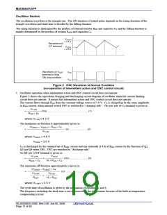
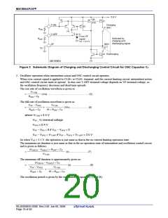
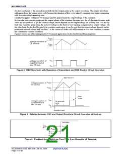
M51995AP/AFP
Current Limiting Section
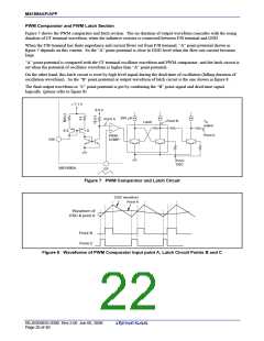
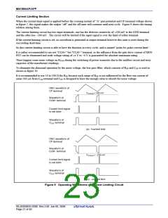
When the current-limit signal is applied before the crossing instant of “A” pint potential and CF terminal voltage shown
in figure 7, this signal makes the output “off” and the off state will continue until next cycle. Figure 9 shows the timing
relation among them.
The current limiting circuit has two input terminals, one has the detector-sensitivity of +200 mV to the GND terminal
and the other has −200 mV. The circuit will be latched if the input signal is over the limit of either terminal.
If the current limiting circuit is set, no waveform is generated at output terminal however this state is reset during the
succeeding dead-time.
So this current limiting circuit is able to have the function in every cycle, and is named “pulse-by-pulse current limit”.
It is rather recommended to use not "CLM+" but "CLM−" terminal, as the influence from the gate drive current of MOS
FET can be eliminated and wide voltage rating of +4 V to −4 V is guaranteed for absolute maximum rating.
There happen some noise voltage on RCLM during the switching of power transistor due to the snubber circuit and stray
capacitor of the transformer windings.
To eliminate the abnormal operation by the noise voltage, the low pass filter, which consists of RNF and CNF is used as
shown in figure 10.
It is recommended to use 10 to 100 Ω for RNF because such range of RNF is not influenced by the flow-out current of
some 200 µA from CLM terminal and CNF is designed to have the enough value to absorb the noise voltage.
OSC waveform of
CF terminal
VTHCLM ≈ 200 mV
Waveform of
CLM+ terminal
Current limit signal
to set latch
Waveform of
VOUT terminal
(a) +current limit
OSC waveform of
CF terminal
Waveform of
CLM− terminal
V
THCLM ≈ −200 mV
Current limit signal
to set latch
Waveform of
VOUT terminal
(b) −current limit
Figure 9 Operating Waveforms of Current Limiting Circuit
REJ03D0835-0300 Rev.3.00 Jun 06, 2008
Page 21 of 40

 RENESAS [ RENESAS TECHNOLOGY CORP ]